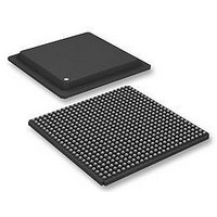
XC6SLX150-2FGG484I Xilinx Inc, XC6SLX150-2FGG484I Datasheet - Page 13

XC6SLX150-2FGG484I
Manufacturer Part Number
XC6SLX150-2FGG484I
Description
FPGA Spartan®-6 Family 147443 Cells 45nm (CMOS) Technology 1.2V 484-Pin FBGA
Manufacturer
Xilinx Inc
Series
Spartan® 6 LXr
Datasheet
1.XC6SLX45-2FGG484CES.pdf
(76 pages)
Specifications of XC6SLX150-2FGG484I
Package
484FBGA
Family Name
Spartan®-6
Device Logic Cells
147443
Device Logic Units
92152
Number Of Registers
184304
Typical Operating Supply Voltage
1.2 V
Maximum Number Of User I/os
338
Ram Bits
4939776
Package / Case
484-BGA
Mounting Type
Surface Mount
Voltage - Supply
1 V ~ 3.6 V
Operating Temperature
-40°C ~ 100°C
Number Of I /o
338
Number Of Logic Elements/cells
147443
No. Of Logic Blocks
23038
No. Of Macrocells
147443
Family Type
Spartan-6
No. Of Speed Grades
2
Total Ram Bits
4939776
No. Of I/o's
338
Clock Management
DCM, PLL
Rohs Compliant
Yes
Lead Free Status / RoHS Status
Lead free / RoHS Compliant
Number Of Gates
-
Lead Free Status / RoHS Status
Lead free / RoHS Compliant
Available stocks
Company
Part Number
Manufacturer
Quantity
Price
Company:
Part Number:
XC6SLX150-2FGG484I
Manufacturer:
XILINX
Quantity:
291
Company:
Part Number:
XC6SLX150-2FGG484I
Manufacturer:
Xilinx Inc
Quantity:
10 000
GTP Transceiver DC Input and Output Levels
Table 16
ended output voltage swing.
Consult UG386: Spartan-6 FPGA GTP Transceivers User Guide for further details.
Table 16: GTP Transceiver DC Specifications
X-Ref Target - Figure 1
X-Ref Target - Figure 2
Table 17
Transceivers User Guide for further details.
DS162 (v2.0) March 31, 2011
Preliminary Product Specification
Notes:
1.
2.
+V
V
0
DV
The output swing and preemphasis levels are programmable using the attributes discussed in the Spartan-6 FPGA GTP Transceivers User Guide
and can result in values lower than reported in this table.
Other values can be used as appropriate to conform to specific protocols and standards.
Symbol
T
V
CMOUTDC
DV
+V
–V
V
R
OSKEW
C
SEOUT
0
V
R
CMIN
PPOUT
OUT
EXT
PPIN
IN
IN
summarizes the DC output specifications of the GTP transceivers in Spartan-6 FPGAs.
summarizes the DC specifications of the clock input of the GTP transceiver. Consult the Spartan-6 FPGA GTP
N
P
P–N
Differential peak-to-peak input
voltage
Absolute input voltage
Common mode input voltage
Differential peak-to-peak output
voltage
Single-ended output voltage swing
Common mode output voltage
Differential input resistance
Differential output resistance
Transmitter output skew
Recommended external AC coupling capacitor
(1)
DC Parameter
Figure 2
Figure 1: Single-Ended Peak-to-Peak Voltage
shows the peak-to-peak differential output voltage.
Figure 2: Differential Peak-to-Peak Voltage
DC coupled
External AC coupled
MGTAVTTRX = 1.2V
DC coupled
MGTAVTTRX = 1.2V
Transmitter output swing is set
to maximum setting
Equation based
(1)
www.xilinx.com
Spartan-6 FPGA Data Sheet: DC and Switching Characteristics
Conditions
(2)
–400
Min
140
80
80
75
–
–
–
–
MGTAVTTTX – V
MGTAVTTRX
Typ
100
100
100
3/4
–
–
–
–
–
Figure 1
SEOUT
MGTAVTTRX
shows the single-
/2
2000
1000
Max
500
130
130
200
Differential
ds162_02_112009
15
–
Voltage
Single-Ended
Voltage
ds162_01_112009
Units
mV
mV
mV
mV
mV
mV
nF
ps
13


