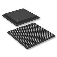
XC6SLX150-2FGG484I Xilinx Inc, XC6SLX150-2FGG484I Datasheet - Page 72

XC6SLX150-2FGG484I
Manufacturer Part Number
XC6SLX150-2FGG484I
Description
FPGA Spartan®-6 Family 147443 Cells 45nm (CMOS) Technology 1.2V 484-Pin FBGA
Manufacturer
Xilinx Inc
Series
Spartan® 6 LXr
Datasheet
1.XC6SLX45-2FGG484CES.pdf
(76 pages)
Specifications of XC6SLX150-2FGG484I
Package
484FBGA
Family Name
Spartan®-6
Device Logic Cells
147443
Device Logic Units
92152
Number Of Registers
184304
Typical Operating Supply Voltage
1.2 V
Maximum Number Of User I/os
338
Ram Bits
4939776
Package / Case
484-BGA
Mounting Type
Surface Mount
Voltage - Supply
1 V ~ 3.6 V
Operating Temperature
-40°C ~ 100°C
Number Of I /o
338
Number Of Logic Elements/cells
147443
No. Of Logic Blocks
23038
No. Of Macrocells
147443
Family Type
Spartan-6
No. Of Speed Grades
2
Total Ram Bits
4939776
No. Of I/o's
338
Clock Management
DCM, PLL
Rohs Compliant
Yes
Lead Free Status / RoHS Status
Lead free / RoHS Compliant
Number Of Gates
-
Lead Free Status / RoHS Status
Lead free / RoHS Compliant
Available stocks
Company
Part Number
Manufacturer
Quantity
Price
Company:
Part Number:
XC6SLX150-2FGG484I
Manufacturer:
XILINX
Quantity:
291
Company:
Part Number:
XC6SLX150-2FGG484I
Manufacturer:
Xilinx Inc
Quantity:
10 000
Table 76: Package Skew (Cont’d)
Table 77: Sample Window
DS162 (v2.0) March 31, 2011
Preliminary Product Specification
Notes:
1.
2.
Notes:
1.
2.
3.
T
T
T
PKGSKEW
SAMP
SAMP_BUFIO2
These values represent the worst-case skew between any two SelectIO resources in the package: shortest delay to longest delay from Pad to Ball.
Some of these devices are available in both Pb and Pb-free (additional G) packages as standard ordering options.
LXT devices are not available with a -1L speed grade.
This parameter indicates the total sampling error of Spartan-6 FPGA DDR input registers, measured across voltage, temperature, and process. The
characterization methodology uses the DCM to capture the DDR input registers’ edges of operation. These measurements include:
- CLK0 DCM jitter
- DCM accuracy (phase offset)
- DCM phase shift resolution
These measurements do not include package or clock tree skew.
This parameter indicates the total sampling error of Spartan-6 FPGA DDR input registers, measured across voltage, temperature, and process. The
characterization methodology uses the BUFIO2 clock network and IODELAY2 to capture the DDR input registers’ edges of operation. These
measurements do not include package or clock tree skew.
Symbol
Symbol
Sampling Error at Receiver Pins
Sampling Error at Receiver Pins using
BUFIO2
Package Skew
(3)
Description
Description
(1)
(2)
www.xilinx.com
Spartan-6 FPGA Data Sheet: DC and Switching Characteristics
XC6SLX150
XC6SLX150T
Device
All
All
Device
(1)
510
430
-3
Package
FG(G)484
FG(G)676
FG(G)900
FG(G)484
FG(G)676
FG(G)900
CSG484
CSG484
510
430
-3N
Speed Grade
(2)
530
450
-2
Value
103
115
121
141
120
84
83
88
740
590
-1L
Units
ps
ps
ps
ps
ps
ps
ps
ps
Units
ps
ps
72


