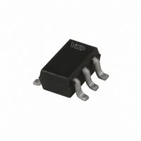
PUMD3,165 NXP Semiconductors, PUMD3,165 Datasheet - Page 4

PUMD3,165
Manufacturer Part Number
PUMD3,165
Description
TRANS NPN/PNP 50V 100MA SOT363
Manufacturer
NXP Semiconductors
Datasheet
1.PUMD3165.pdf
(11 pages)
Specifications of PUMD3,165
Package / Case
SC-70-6, SC-88, SOT-363
Transistor Type
1 NPN, 1 PNP - Pre-Biased (Dual)
Current - Collector (ic) (max)
100mA
Voltage - Collector Emitter Breakdown (max)
50V
Resistor - Base (r1) (ohms)
10K
Resistor - Emitter Base (r2) (ohms)
10K
Dc Current Gain (hfe) (min) @ Ic, Vce
30 @ 5mA, 5V
Vce Saturation (max) @ Ib, Ic
150mV @ 500µA, 10mA
Current - Collector Cutoff (max)
1µA
Power - Max
300mW
Mounting Type
Surface Mount
Configuration
Dual
Transistor Polarity
NPN/PNP
Typical Input Resistor
10 KOhms
Typical Resistor Ratio
1
Mounting Style
SMD/SMT
Collector- Emitter Voltage Vceo Max
50 V
Peak Dc Collector Current
100 mA
Maximum Operating Temperature
+ 150 C
Minimum Operating Temperature
- 65 C
Lead Free Status / RoHS Status
Lead free / RoHS Compliant
Frequency - Transition
-
Lead Free Status / RoHS Status
Lead free / RoHS Compliant, Lead free / RoHS Compliant
Other names
934050170165
PUMD3 /T2
PUMD3 /T2
PUMD3 /T2
PUMD3 /T2
Available stocks
Company
Part Number
Manufacturer
Quantity
Price
Part Number:
PUMD3,165
Manufacturer:
NEXPERIA/安世
Quantity:
20 000
NXP Semiconductors
6. Thermal characteristics
7. Characteristics
PEMD3_PIMD3_PUMD3_10
Product data sheet
Table 7.
[1]
[2]
[3]
Table 8.
T
Symbol
Per transistor
R
Per device
R
Symbol Parameter
Per transistor; for the PNP transistor with negative polarity
I
I
I
h
V
V
V
R1
R2/R1
C
CBO
CEO
EBO
amb
FE
CEsat
I(off)
I(on)
th(j-a)
th(j-a)
c
Device mounted on an FR4 PCB, single-sided copper, tin-plated and standard footprint.
Device mounted on an FR4 PCB with 65 μm copper strip line, standard footprint.
Reflow soldering is the only recommended soldering method.
= 25
°
collector-base cut-off
current
collector-emitter
cut-off current
emitter-base cut-off
current
DC current gain
collector-emitter
saturation voltage
off-state input voltage V
on-state input voltage V
bias resistor 1 (input)
bias resistor ratio
collector capacitance V
C unless otherwise specified.
Parameter
thermal resistance from
junction to ambient
thermal resistance from
junction to ambient
Thermal characteristics
Characteristics
TR1 (NPN)
TR2 (PNP)
SOT363
SOT457
SOT666
SOT363
SOT457
SOT666
Rev. 10 — 15 November 2009
NPN/PNP resistor-equipped transistors; R1 = 10 kΩ, R2 = 10 kΩ
Conditions
V
V
V
T
V
V
I
f = 1 MHz
C
j
CB
CE
CE
EB
CE
CE
CE
CB
= 150 °C
= 10 mA; I
Conditions
in free air
in free air
= 50 V; I
= 30 V; I
= 30 V; I
= 5 V; I
= 5 V; I
= 5 V; I
= 0.3 V; I
= 10 V; I
PEMD3; PIMD3; PUMD3
C
C
C
E
B
B
B
E
= 0 A
= 5 mA
= 100 μA
C
= 0.5 mA
= 0 A
= 0 A
= 0 A;
= i
= 10 mA
e
= 0 A;
[1][3]
[1][3]
[1]
[2]
[1]
[2]
Min
-
-
-
-
-
-
Min
-
-
-
-
30
-
-
2.5
7
0.8
-
-
-
Typ
-
-
-
-
-
-
Typ
-
-
-
-
-
-
1.1
1.8
10
1
-
-
-
© NXP B.V. 2009. All rights reserved.
Max
625
417
625
416
208
416
Max
100
1
50
400
-
150
0.8
-
13
1.2
-
2.5
3
Unit
K/W
K/W
K/W
K/W
K/W
K/W
Unit
nA
μA
μA
μA
V
V
kΩ
pF
pF
mV
4 of 11


