NST3904F3T5G ON Semiconductor, NST3904F3T5G Datasheet

TRANSISTOR NPN 40V 0.2A SOT1123

NST3904F3T5G

Manufacturer Part Number
NST3904F3T5G
Description
TRANSISTOR NPN 40V 0.2A SOT1123
Manufacturer
ON Semiconductor
Datasheet

Specifications of NST3904F3T5G

Transistor Type
NPN
Current - Collector (ic) (max)
200mA
Voltage - Collector Emitter Breakdown (max)
40V
Vce Saturation (max) @ Ib, Ic
300mV @ 5mA, 50mA
Dc Current Gain (hfe) (min) @ Ic, Vce
100 @ 10mA, 1V
Power - Max
290mW
Frequency - Transition
200MHz
Mounting Type
Surface Mount
Package / Case
SOT-1123
Configuration
Single
Transistor Polarity
NPN
Mounting Style
SMD/SMT
Collector- Emitter Voltage Vceo Max
40 V
Emitter- Base Voltage Vebo
6 V
Maximum Dc Collector Current
0.2 A
Power Dissipation
347 mW
Maximum Operating Frequency
200 MHz
Maximum Operating Temperature
+ 150 C
Minimum Operating Temperature
- 55 C
Lead Free Status / RoHS Status
Lead free / RoHS Compliant
Current - Collector Cutoff (max)
-
Lead Free Status / Rohs Status
Lead free / RoHS Compliant
Other names
NST3904F3T5G
NST3904F3T5GOSTR

Available stocks

Company
Part Number
Manufacturer
Quantity
Price
Part Number:
NST3904F3T5G
Manufacturer:
ON Semiconductor
Quantity:
5 550
Part Number:
NST3904F3T5G
Manufacturer:
ON/安森美
Quantity:
20 000
NST3904F3T5G
NPN General Purpose
Transistor
SOT−23/SOT−323/SOT−563/SOT−963 three−leaded device. It is
designed for general purpose amplifier applications and is housed in
the SOT−1123 surface mount package. This device is ideal for
low−power surface mount applications where board space is at a
premium.
Features
Stresses exceeding Maximum Ratings may damage the device. Maximum
Ratings are stress ratings only. Functional operation above the Recommended
Operating Conditions is not implied. Extended exposure to stresses above the
Recommended Operating Conditions may affect device reliability.
1. 100 mm
2. 500 mm
© Semiconductor Components Industries, LLC, 2008
April, 2008 − Rev. 0
MAXIMUM RATINGS
THERMAL CHARACTERISTICS
Collector −Emitter Voltage
Collector −Base Voltage
Emitter −Base Voltage
Collector Current − Continuous
Junction and Storage Temperature Range
Total Device Dissipation, T
Thermal Resistance,
Total Device Dissipation, T
Thermal Resistance,
Thermal Resistance,
The NST3904F3T5G device is a spin−off of our popular
h
Low V
Reduces Board Space
This is a Pb−Free Device
FE
Derate above 25°C
Junction−to−Ambient
Derate above 25°C
Junction−to−Ambient
Junction−to−Lead 3
, 100−300
CE(sat)
2
2
1 oz, copper traces.
Characteristic
, ≤ 0.4 V
Rating
A
A
= 25°C
= 25°C
Symbol
Symbol
(Note 1)
(Note 1)
(Note 2)
(Note 2)
(Note 2)
T
V
V
V
R
R
R
J
P
P
CEO
CBO
EBO
, T
I
YJL
qJA
qJA
C
D
D
stg
−55 to
Value
+150
Max
200
290
432
347
360
143
6.0
2.3
2.8
40
60
1
mW/°C
mW/°C
mAdc
°C/W
°C/W
°C/W
Unit
Unit
Vdc
Vdc
Vdc
mW
mW
°C
†For information on tape and reel specifications,
NST3904F3T5G
including part orientation and tape sizes, please
refer to our Tape and Reel Packaging Specifications
Brochure, BRD8011/D.
Device
ORDERING INFORMATION
BASE
MARKING DIAGRAM
http://onsemi.com
2
M
1
3
NST3904F3T5G
CASE 524AA
SOT−1123
= Device Code
= Date Code
STYLE 1
SOT−1123
(Pb−Free)
COLLECTOR
Package
EMITTER
2 M
Publication Order Number:
1
1
3
2
2
8000/Tape & Reel
NST3904F3/D
Shipping

Related parts for NST3904F3T5G

NST3904F3T5G Summary of contents

Page 1

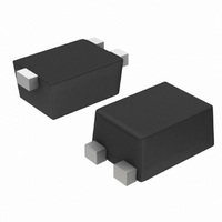
... NST3904F3T5G NPN General Purpose Transistor The NST3904F3T5G device is a spin−off of our popular SOT−23/SOT−323/SOT−563/SOT−963 three−leaded device designed for general purpose amplifier applications and is housed in the SOT−1123 surface mount package. This device is ideal for low−power surface mount applications where board space premium ...

Page 2

ELECTRICAL CHARACTERISTICS Characteristic OFF CHARACTERISTICS Collector −Emitter Breakdown Voltage (Note 3) (I Collector −Base Breakdown Voltage ( mAdc Emitter −Base Breakdown Voltage ( mAdc Collector Cutoff Current ( Vdc, V ...

Page 3

1.0 0.9 −55°C 0.8 0.7 25°C 0.6 0.5 150°C 0.4 0.3 0.0001 0.001 0. COLLECTOR CURRENT (A) C Figure 3. Base Emitter Saturation Voltage vs. Collector Current 2.0 1 ...

Page 4

... SOLDERING FOOTPRINT* 0.35 0.30 0.25 0.90 DIMENSIONS: MILLIMETERS details, please download the ON Semiconductor Soldering and Mounting Techniques Reference Manual, SOLDERRM/D. N. American Technical Support: 800−282−9855 Toll Free USA/Canada Europe, Middle East and Africa Technical Support: Phone: 421 33 790 2910 Japan Customer Focus Center Phone: 81− ...

Related keywords