2N5194G ON Semiconductor, 2N5194G Datasheet - Page 4
2N5194G
Manufacturer Part Number
2N5194G
Description
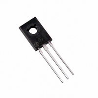
TRANS PNP PWR GP 4A 60V TO225AA
Manufacturer
ON Semiconductor
Type
Powerr
Specifications of 2N5194G
Transistor Type
PNP
Current - Collector (ic) (max)
4A
Voltage - Collector Emitter Breakdown (max)
60V
Vce Saturation (max) @ Ib, Ic
1.4V @ 1A, 4A
Current - Collector Cutoff (max)
1mA
Dc Current Gain (hfe) (min) @ Ic, Vce
25 @ 1.5A, 2V
Power - Max
40W
Frequency - Transition
2MHz
Mounting Type
Through Hole
Package / Case
TO-225-3
Current, Collector
4 A
Current, Gain
10
Frequency
2 MHz
Package Type
TO-225AA
Polarity
PNP
Power Dissipation
40 W
Primary Type
Si
Resistance, Thermal, Junction To Case
3.12 °C/W
Voltage, Breakdown, Collector To Emitter
60 V
Voltage, Collector To Base
60 V
Voltage, Collector To Emitter
60 V
Voltage, Collector To Emitter, Saturation
1.4 V
Voltage, Emitter To Base
5 V
Lead Free Status / RoHS Status
Lead free / RoHS Compliant
Other names
2N5194GOS
Available stocks
Company
Part Number
Manufacturer
Quantity
Price


APPROX
V
APPROX
−11 V
BE(off)
5.0
2.0
1.0
0.5
0.2
0.1
−11 V
0.07
0.05
0.03
0.02
10
Figure 7. Switching Time Equivalent Test Circuit
2.0
1.0
0.7
0.5
0.3
0.2
0.1
V
1.0
in
0.05
V
in
0
TURN−OFF PULSE
CURVES APPLY BELOW RATED V
0.07 0.1
TURN−ON PULSE
t
d
T
J
2.0
@ V
Figure 11. Rating and Thermal Data
Active−Region Safe Operating Area
V
= 150°C
t
CE
2
t
t
1
r
BE(off)
SECONDARY BREAKDOWN LIMIT
THERMAL LIMIT @ T
BONDING WIRE LIMIT
@ V
, COLLECTOR−EMITTER VOLTAGE (VOLTS)
t
r
@ V
CC
t
I
= 2.0 V
3
C
Figure 9. Turn−On Time
, COLLECTOR CURRENT (AMP)
= 10 V
CC
5.0
0.2
= 30 V
APPROX
0.3
+9.0 V
DUTY CYCLE ≈ 2.0%
5.0 ms
100 < t
10
C
t
t
1
V
C
3
= 25°C
0.5
V
CC
≤ 7.0 ns
jd
< 15 ns
in
2
CEO
dc
<< C
< 500 ms
0.7
1.0 ms
20
R
2N5194
2N5195
eb
R
B
+4.0 V
R
TO OBTAIN DESIRED
CURRENT LEVELS
C
B
1.0
AND R
I
T
C
J
/I
C
= 25°C
B
50
VARIED
= 10
2.0
100 ms
2N5194, 2N5195
http://onsemi.com
SCOPE
3.0
100
4.0
4
Note 1:
a transistor; average junction temperature and second
breakdown. Safe operating area curves indicate I
limits of the transistor that must be observed for reliable
operation; i.e., the transistor must not be subjected to greater
dissipation than the curves indicate.
variable depending on conditions. Second breakdown pulse
limits are valid for duty cycles to 10% provided T
v 150_C. At high−case temperatures, thermal limitations
will reduce the power that can be handled to values less than
the limitations imposed by second breakdown.
500
300
200
100
0.07
0.05
0.03
0.02
There are two limitations on the power handling ability of
The data of Figure 11 is based on T
70
50
2.0
1.0
0.7
0.5
0.3
0.2
0.1
0.1
0.05
0.07 0.1
0.2 0.3 0.5
t
f
t
s
@ V
′
V
Figure 10. Turn−Off Time
I
R
C
Figure 8. Capacitance
, REVERSE VOLTAGE (VOLTS)
CC
, COLLECTOR CURRENT (AMP)
0.2
= 10 V
1.0
t
f
0.3
@ V
2.0
CC
= 30 V
0.5
3.0
0.7
C
5.0
eb
J(pk)
1.0
= 150_C. T
10
I
I
t
T
B1
C
s
J
′ = t
/I
= 25°C
B
= I
T
= 10
J
2.0
s
B2
= 25°C
20
− 1/8 t
C
3.0
C
− V
30
cb
f
J(pk)
4.0
C
40
CE
is
Related parts for 2N5194G
Image
Part Number
Description
Manufacturer
Datasheet
Request
R

Part Number:
Description:
ON Semiconductor [VOLTAGE REGULATOR]
Manufacturer:
ON Semiconductor
Datasheet:
Part Number:
Description:
357-036-542-201 CARDEDGE 36POS DL .156 BLK LOPRO
Manufacturer:
ON Semiconductor
Datasheet:
Part Number:
Description:
357-036-542-201 CARDEDGE 36POS DL .156 BLK LOPRO
Manufacturer:
ON Semiconductor
Datasheet:
Part Number:
Description:
357-036-542-201 CARDEDGE 36POS DL .156 BLK LOPRO
Manufacturer:
ON Semiconductor
Datasheet:
Part Number:
Description:
357-036-542-201 CARDEDGE 36POS DL .156 BLK LOPRO
Manufacturer:
ON Semiconductor
Datasheet:
Part Number:
Description:
357-036-542-201 CARDEDGE 36POS DL .156 BLK LOPRO
Manufacturer:
ON Semiconductor
Datasheet:
Part Number:
Description:
357-036-542-201 CARDEDGE 36POS DL .156 BLK LOPRO
Manufacturer:
ON Semiconductor
Datasheet:
Part Number:
Description:
357-036-542-201 CARDEDGE 36POS DL .156 BLK LOPRO
Manufacturer:
ON Semiconductor
Datasheet:
Part Number:
Description:
357-036-542-201 CARDEDGE 36POS DL .156 BLK LOPRO
Manufacturer:
ON Semiconductor
Datasheet:
Part Number:
Description:
357-036-542-201 CARDEDGE 36POS DL .156 BLK LOPRO
Manufacturer:
ON Semiconductor
Datasheet:
Part Number:
Description:
357-036-542-201 CARDEDGE 36POS DL .156 BLK LOPRO
Manufacturer:
ON Semiconductor
Datasheet:
Part Number:
Description:
Manufacturer:
ON Semiconductor
Datasheet:
Part Number:
Description:
Manufacturer:
ON Semiconductor
Datasheet:
Part Number:
Description:
Manufacturer:
ON Semiconductor
Datasheet: