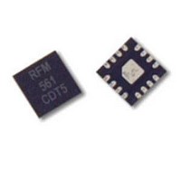
TXC100 RFM, TXC100 Datasheet - Page 3
TXC100
Manufacturer Part Number
TXC100
Description
RF Transceiver Transmitter 300-450MHz ASK/FSK
Manufacturer
RFM
Datasheet
1.TXC100.pdf
(11 pages)
Specifications of TXC100
Output Power
- 10 dBm to + 10 dBm
Operating Supply Voltage
2.5 V, 3.3 V
Mounting Style
SMD/SMT
Package / Case
TQFN-16
Minimum Operating Temperature
- 40 C
Lead Free Status / RoHS Status
Lead free / RoHS Compliant


Pin Configuration
Pin Description
www.RFM.com
©RF Monolithics, Inc.
Pin
1
2
3
4
Name
V
Mode
Stdby
Data
Email:
DD
IN
Sel
info@rfm.com
Description
V
capacitors.
The Mode Select Pin allows the TXC100 to be set in either OOK/ASK or FSK mode:
In OOK/ASK mode, data input to the Data
low turns off the power amplifier.
In FSK mode, data input to the Data
A logic low performs no shift. The frequency of a logic low input in FSK mode is the same frequency as a logic high in OOK/ASK mode.
The FSK deviation is achieved by pulling the crystal frequency. See Crystal Reference section (pin 15) for more details. The maximum
FSK deviation for the 315 MHz band and 433 MHz band is approximately 55 kHz and 80 kHz, respectively.
The Data Input Pin turns the Power Amplifier on/off in OOK/ASK mode, or high/low frequency in FSK mode:
Low (OOK/ASK mode): Power Amplifier off
High (OOK/ASK mode): Power Amplifier on
Low (FSK mode): Low frequency
High (FSK mode): High frequency
The Standby Input Pin selects active or low power shutdown/standby mode:
If this pin unconnected or logic low, the TXC100 is placed in low current standby mode.
If this pin is logic high, the TXC100 is in active mode and ready to transmit
Note: Lowest current consumption is achieved when all configuration pins are logic low.
When this pin sets the device in low power shutdown, the device draws nominally 0.2 nA. When the device is brought out of standby with
a logic high input, it is ready for operation within 200 µs. This pin has an internal pull-down resistor so it can be pulled low or left
unconnected.The 200 µs turn-on time is due to crystal start-up. An optimally matched crystal will minimize this turn-on time. See the
Crystal Reference section (Pin 15) for details on crystal load matching.
DD
Logic Low: OOK/ASK mode
Logic High: FSK mode
is the supply voltage for the PLL and logic circuitry. Bypass this pin as close as possible with parallel 1.0 µF, 0.01 µF, 220 pF
BOTTOM VIEW
3x3mm
Dev0
Dev1
Clk0
Clk1
12
11
10
9
IN
Pin shifts the carrier frequency by the amount programmed through the DEV[2..0] pins (11,12,13).
IN
13
8
Pin (3) gates the internal power amplifier. A logic high turns the power amplifier on. A logic
14
7
15
6
16
5
1
2
3
4
V
Mode
Data
Stdby
DD
IN
Sel
TXC100 - 08/18/10
Page 3 of 11
Related parts for TXC100
Image
Part Number
Description
Manufacturer
Datasheet
Request
R

Part Number:
Description:
TX/RX ASK/FSK 868-870MHZ 38TSSOP
Manufacturer:
Infineon Technologies
Datasheet:

Part Number:
Description:
ASH RX 115.2 KBPS 433.92 MHZ
Manufacturer:
RFM
Datasheet:

Part Number:
Description:
RFIC TRANCEIVER MULTI-CHANNEL FS
Manufacturer:
RFM
Datasheet:

Part Number:
Description:
ASH TX 115.2 KBPS 433.92 MHZ
Manufacturer:
RFM
Datasheet:
Part Number:
Description:
Filters 1602MHz BW=61MHz
Manufacturer:
RFM
Datasheet:

Part Number:
Description:
RESONATOR, SM3030-6
Manufacturer:
RFM
Datasheet:

Part Number:
Description:
RESONATOR, SM3030-6
Manufacturer:
RFM
Datasheet:

Part Number:
Description:
RESONATOR, SM3030-6
Manufacturer:
RFM
Datasheet:

Part Number:
Description:
RESONATOR, SM5035-4
Manufacturer:
RFM
Datasheet:
Part Number:
Description:
RESONATOR 418MHZ SM5035-4
Manufacturer:
RFM
Datasheet:

Part Number:
Description:
TXC-02050-AIPLMRT Device 6-,8-,34-Mbit Line Interface TXC-0250
Manufacturer:
ETC ETC
Datasheet:

Part Number:
Description:
Manufacturer:
Transwitch Corporation
Datasheet:
Part Number:
Description:
Manufacturer:
Transwitch Corporation
Datasheet: