TXC100 RFM, TXC100 Datasheet - Page 9
TXC100
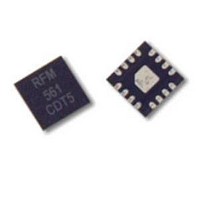
Manufacturer Part Number
TXC100
Description
RF Transceiver Transmitter 300-450MHz ASK/FSK
Manufacturer
RFM
Datasheet
1.TXC100.pdf
(11 pages)
Specifications of TXC100
Output Power
- 10 dBm to + 10 dBm
Operating Supply Voltage
2.5 V, 3.3 V
Mounting Style
SMD/SMT
Package / Case
TQFN-16
Minimum Operating Temperature
- 40 C
Lead Free Status / RoHS Status
Lead free / RoHS Compliant


www.RFM.com
©RF Monolithics, Inc.
Theory of Operation
Introduction
The TXC100 is a crystal-referenced transmitter designed to operate in the 315/433 MHz frequency spectrum. The carrier and crystal reference
relation is given by:
It is capable of supporting ASK and FSK data transmissions at 100 and 20 kbps, respectively. The output power is adjustable from -10 dBm
to +10 dBm thru a resistor at the ES
IC also provides a scaled and buffered clock output of the reference crystal for use by an external processor. The clock output frequency scaling
programmable.
Frequency Synthesizer
The frequency synthesizer is a phase locked loop (PLL) circuit with a loop bandwidth of 300 kHz. The PLL contains a phase detector, charge pump,
VCO, integrated loop filter, ÷32 clock divider, and crystal oscillator drive circuit. The internal PLL is self contained and requires no external
components for filtering or dividing. Only a reference crystal is needed.
50Ω Ω Ω Ω Output Matching
When properly matched, the TXC100 can output up to +12 dBm into a 50Ω load. The output is an open-drain configuration which requires a pull-up
inductor for biasing. The pull-up inductance serves to provide biasing for the power amplifier and is a high frequency choke to reduce unwanted
coupling back into the power supply. Maximum power transfer occurs when the output is closely matched to 250Ω. For best performance use
wirewound inductors instead of chip inductors. Wirewound inductors provide lower insertion loss as opposed to chip inductors. See Typical
Application Circuit (section IV) for topology and matching component values.
PCB Layout Considerations
PCB layout is critical to proper and consistent operation. Always use controlled impedance lines from the PA
a 50Ω impedance line is approximately 0.110” wide. Component spacing is critical as well. Keep all output matching components as close together
as possible to minimize stray inductance and capacitance that can detune the matching network. Keep top side ground planes at least a board
thickness away from the signal output leading to the antenna or RF connector.
Email:
info@rfm.com
OUT
(pin 7). The FSK frequency deviation is programmable with up to eight different deviation values. The
f
C
= f
XTAL
* 32
OUT
(pin 8). For a .062” thick FR4 board,
TXC100 - 08/18/10
Page 9 of 11
Related parts for TXC100
Image
Part Number
Description
Manufacturer
Datasheet
Request
R

Part Number:
Description:
TX/RX ASK/FSK 868-870MHZ 38TSSOP
Manufacturer:
Infineon Technologies
Datasheet:

Part Number:
Description:
ASH RX 115.2 KBPS 433.92 MHZ
Manufacturer:
RFM
Datasheet:

Part Number:
Description:
RFIC TRANCEIVER MULTI-CHANNEL FS
Manufacturer:
RFM
Datasheet:

Part Number:
Description:
ASH TX 115.2 KBPS 433.92 MHZ
Manufacturer:
RFM
Datasheet:
Part Number:
Description:
Filters 1602MHz BW=61MHz
Manufacturer:
RFM
Datasheet:

Part Number:
Description:
RESONATOR, SM3030-6
Manufacturer:
RFM
Datasheet:

Part Number:
Description:
RESONATOR, SM3030-6
Manufacturer:
RFM
Datasheet:

Part Number:
Description:
RESONATOR, SM3030-6
Manufacturer:
RFM
Datasheet:

Part Number:
Description:
RESONATOR, SM5035-4
Manufacturer:
RFM
Datasheet:
Part Number:
Description:
RESONATOR 418MHZ SM5035-4
Manufacturer:
RFM
Datasheet:

Part Number:
Description:
TXC-02050-AIPLMRT Device 6-,8-,34-Mbit Line Interface TXC-0250
Manufacturer:
ETC ETC
Datasheet:

Part Number:
Description:
Manufacturer:
Transwitch Corporation
Datasheet:
Part Number:
Description:
Manufacturer:
Transwitch Corporation
Datasheet: