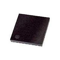
ATA5824-PLQW80 Atmel, ATA5824-PLQW80 Datasheet - Page 66

ATA5824-PLQW80
Manufacturer Part Number
ATA5824-PLQW80
Description
RF Transceiver RF Data Control Duplex Trans.
Manufacturer
Atmel
Datasheet
1.ATA5824-PLQW.pdf
(98 pages)
Specifications of ATA5824-PLQW80
Wireless Frequency
435 MHz
Interface Type
4-Wire SPI
Noise Figure
6.5 dB
Output Power
10 dBm
Operating Supply Voltage
4.4 V to 5.25 V
Maximum Operating Temperature
+ 105 C
Mounting Style
SMD/SMT
Package / Case
QFN-48
Maximum Data Rate
5 Kbps
Minimum Operating Temperature
- 40 C
Modulation
ASK, FSK
Lead Free Status / RoHS Status
Lead free / RoHS Compliant
- Current page: 66 of 98
- Download datasheet (4Mb)
66
ATA5823/ATA5824
The timing of the FD mode is illustrated in
place if the FD mode is enabled in the slave before it is enabled in the master. If the FD mode is
enabled in the master before it is enabled in the slave, a maximum delay T
proper operation. T
during the Bit-check. This is calculated as follows:
T
Table 14-7.
This means, to get a extended time period for enabling the FD mode, increase the preburst
length in the master and reduce N
sampling edge (pin SCK) for the LSB while writing control register 1.
For a proper operation in the slave, a wake-up due to noise must be prevent (bit check + start bit
ok). To achieve this for the slave the following adjustments are recommended:
FD_sync
1. Set N
2. Start FD mode in master and slave as simultaneously as possible.
< T
BIT-check
Preburst
T
Bit-check-min
6 (recommended)
- T
FD_sync
N
6
Startup-sig-proc-fd
Bit-check
3
9
depends on the preburst length and the number of bits to be checked
- T
Bit-check
Bit-check-min
Figure 14-13 on page
in the slave. The reference points for T
67. A proper data transfer takes
10
4
7
T
Bit-check-min
168
168
168
FD_sync
T
T
T
DCLK
DCLK
DCLK
is allowed for a
FD_sync
4829D–RKE–06/06
are the
Related parts for ATA5824-PLQW80
Image
Part Number
Description
Manufacturer
Datasheet
Request
R

Part Number:
Description:
IC TXRX UHF ASK/FSK 48QFN
Manufacturer:
Atmel
Datasheet:

Part Number:
Description:
Manufacturer:
Atmel
Datasheet:

Part Number:
Description:
DEV KIT FOR AVR/AVR32
Manufacturer:
Atmel
Datasheet:

Part Number:
Description:
INTERVAL AND WIPE/WASH WIPER CONTROL IC WITH DELAY
Manufacturer:
ATMEL Corporation
Datasheet:

Part Number:
Description:
Low-Voltage Voice-Switched IC for Hands-Free Operation
Manufacturer:
ATMEL Corporation
Datasheet:

Part Number:
Description:
MONOLITHIC INTEGRATED FEATUREPHONE CIRCUIT
Manufacturer:
ATMEL Corporation
Datasheet:

Part Number:
Description:
AM-FM Receiver IC U4255BM-M
Manufacturer:
ATMEL Corporation
Datasheet:

Part Number:
Description:
Monolithic Integrated Feature Phone Circuit
Manufacturer:
ATMEL Corporation
Datasheet:

Part Number:
Description:
Multistandard Video-IF and Quasi Parallel Sound Processing
Manufacturer:
ATMEL Corporation
Datasheet:

Part Number:
Description:
High-performance EE PLD
Manufacturer:
ATMEL Corporation
Datasheet:

Part Number:
Description:
8-bit Flash Microcontroller
Manufacturer:
ATMEL Corporation
Datasheet:

Part Number:
Description:
2-Wire Serial EEPROM
Manufacturer:
ATMEL Corporation
Datasheet:


