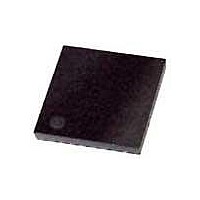
ATA5428-PLQW80 Atmel, ATA5428-PLQW80 Datasheet - Page 37

ATA5428-PLQW80
Manufacturer Part Number
ATA5428-PLQW80
Description
RF Transceiver ASK/FSK Transceiver 434 and 868MHz
Manufacturer
Atmel
Datasheet
1.ATAB5428-8-WB.pdf
(100 pages)
Specifications of ATA5428-PLQW80
Wireless Frequency
226 KHz, 237 KHz
Interface Type
4-Wire SPI
Noise Figure
7 dB
Output Power
10 dBm
Operating Supply Voltage
2.4 V to 3.6 V
Maximum Operating Temperature
+ 85 C
Mounting Style
SMD/SMT
Package / Case
QFN-48
Maximum Data Rate
20 Kbps
Minimum Operating Temperature
- 40 C
Modulation
ASK, FSK
Lead Free Status / RoHS Status
Lead free / RoHS Compliant
- Current page: 37 of 100
- Download datasheet (2Mb)
7.2
4841D–WIRE–10/07
TX/RX Data Buffer
After the transceiver is turned on via pin PWR_ON = High, T1 = Low, T2 = Low, T3 = Low,
T4 = Low or T5 = Low or the voltage at pin VAUX V
are in the default state.
Figure 7-1.
The TX/RX data buffer is used to handle the data transfer during RX and TX operations.
BitChk
NFSK
FR12
MSB
ASK/
Baud
FR6
ST5
IR1
1
1
Register Structure
BitChk
Sleep
FR11
Baud
FR5
ST4
IR0
4
0
0
ATA5423/ATA5425/ATA5428/ATA5429
AVCC
FR10
Sleep
max5
Lim_
min5
Lim_
_EN
FR4
ST3
3
Sleep
max4
Lim_
min4
Lim_
FR3
FR9
ST2
FS
2
Sleep
max3
Lim_
min3
Lim_
FR2
FR8
ST1
1
-
Power_
OPM1 OPM0
Sleep
max2
Lim_
min2
Lim_
FR1
FR7
On
0
VSOUT
XSleep
max1
Low_
Lim_
min1
Lim_
_EN
FR0
Batt
VAUX
MODE
MODE
P_On
CLK_
max0
XLim
_Aux
Lim_
min0
Lim_
LSB
ON
T_
P_
> 3.5V (typically), the control registers
Control Register 1 (ADR 0)
Control Register 2 (ADR 1)
Control Register 3 (ADR 2)
Control Register 4 (ADR 3)
Control Register 5 (ADR 4)
Control Register 6 (ADR 5)
Status Register (ADR 8)
TX/RX Data Buffer:
16
8 Bit
37
Related parts for ATA5428-PLQW80
Image
Part Number
Description
Manufacturer
Datasheet
Request
R

Part Number:
Description:
IC TXRX WIDEBND 433/868MHZ 48QFN
Manufacturer:
Atmel
Datasheet:

Part Number:
Description:
RF Transceiver ASK/FSK Transceiver 434 and 868MHz
Manufacturer:
Atmel
Datasheet:

Part Number:
Description:
RF Transceiver ASK/FSK Transceiver 434 and 868 MHz
Manufacturer:
Atmel
Datasheet:

Part Number:
Description:
Manufacturer:
Atmel
Datasheet:

Part Number:
Description:
Manufacturer:
Atmel
Datasheet:

Part Number:
Description:
Uhf Ask/fsk Transceiver
Manufacturer:
ATMEL Corporation
Datasheet:

Part Number:
Description:
DEV KIT FOR AVR/AVR32
Manufacturer:
Atmel
Datasheet:

Part Number:
Description:
INTERVAL AND WIPE/WASH WIPER CONTROL IC WITH DELAY
Manufacturer:
ATMEL Corporation
Datasheet:

Part Number:
Description:
Low-Voltage Voice-Switched IC for Hands-Free Operation
Manufacturer:
ATMEL Corporation
Datasheet:

Part Number:
Description:
MONOLITHIC INTEGRATED FEATUREPHONE CIRCUIT
Manufacturer:
ATMEL Corporation
Datasheet:

Part Number:
Description:
AM-FM Receiver IC U4255BM-M
Manufacturer:
ATMEL Corporation
Datasheet:

Part Number:
Description:
Monolithic Integrated Feature Phone Circuit
Manufacturer:
ATMEL Corporation
Datasheet:


