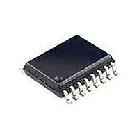
CY2308SC-1HT Cypress Semiconductor Corp, CY2308SC-1HT Datasheet

CY2308SC-1HT
Specifications of CY2308SC-1HT
Available stocks
Related parts for CY2308SC-1HT
CY2308SC-1HT Summary of contents
Page 1
... Logic Block Diagram REF /2 Extra Divider (–5H Cypress Semiconductor Corporation Document Number: 38-07146 Rev. *E Input Decoding” required, Bank B is three-stated. The input clock is directly applied to the output for chip and system testing purposes by the select inputs. The CY2308 PLL enters a power down state when there are no rising edges on the REF input ...
Page 2
Pinouts Table 1. Pin Definitions - 16 Pin SOIC Pin Signal [1] 1 REF [2] 2 CLKA1 [2] 3 CLKA2 GND [2] 6 CLKB1 [2] 7 CLKB2 [ [ [2] 10 CLKB3 ...
Page 3
Available CY2308 Configurations Device Feedback From CY2308–1 Bank A or Bank B CY2308–1H Bank A or Bank B CY2308–2 Bank A CY2308–2 Bank B CY2308–3 Bank A CY2308–3 Bank B CY2308–4 Bank A or Bank B CY2308–5H Bank A or ...
Page 4
Maximum Ratings Supply Voltage to Ground Potential................–0.5V to +7.0V DC Input Voltage (Except Ref) .............. –0. Input Voltage REF ........................................... –0 Operating Conditions for Commercial Temperature Devices Parameter V Supply Voltage DD T Operating Temperature ...
Page 5
Switching Characteristics for Commercial Temperature Devices Parameter Name t Output Frequency 1 t Output Frequency 1 t Output Frequency 1 ÷ t [7] Duty Cycle = (–1, –2, –3, –4, –1H, –5H) ÷ t [7] Duty Cycle ...
Page 6
Operating Conditions for Industrial Temperature Devices Parameter V Supply Voltage DD T Operating Temperature (Ambient Temperature Load Capacitance, below 100 MHz L Load Capacitance, from 100 MHz to 133 MHz [6] C Input Capacitance IN t Power-up time ...
Page 7
Switching Characteristics for Industrial Temperature Devices Parameter Name t Output Frequency 1 t Output Frequency 1 t Output Frequency 1 ÷ t [7] Duty Cycle = (–1, –2, –3, –4, –1H, –5H) [7] ÷ t Duty Cycle ...
Page 8
Switching Waveforms 1.4V 2.0V OUTPUT 0. 1.4V OUTPUT OUTPUT INPUT FBK t 6 FBK, Device 1 FBK, Device 2 t Document Number: 38-07146 Rev. *E Figure 2. Duty Cycle Timing ...
Page 9
Typical Duty Cycle [10] and I DD Duty Cycle Vs VDD (for 30 pF Loads over Frequency - 3.3V, 25C 3.1 3.2 3.3 3.4 3.5 VDD (V) Duty ...
Page 10
Typical Duty Cycle [10] and I DD Duty Cycle Vs VDD (for 30 pF Loads over Frequency - 3.3V, 25C 3.1 3.2 3.3 3.4 3.5 VDD (V) Duty ...
Page 11
Test Circuits Test Circuit 0.1 μF Outputs V DD 0.1 μF GND GND Test Circuit for all parameters except t Document Number: 38-07146 Rev. *E Test Circuit 0.1 μF CLK OUT C LOAD V ...
Page 12
... SOIC CY2308SI–2T 16-pin 150 mil SOIC - Tape and Reel CY2308SC–3 16-pin 150 mil SOIC CY2308SC–3T 16-pin 150 mil SOIC - Tape and Reel CY2308SC–4 16-pin 150 mil SOIC CY2308SC–4T 16-pin 150 mil SOIC - Tape and Reel CY2308SI– ...
Page 13
Ordering Information (continued) Ordering Code CY2308SXI–3 16-pin 150 mil SOIC CY2308SXI–3T 16-pin 150 mil SOIC -Tape and Reel CY2308SXC–4 16-pin 150 mil SOIC CY2308SXC–4T 16-pin 150 mil SOIC - Tape and Reel CY2308SXI–4 16-pin 150 mil SOIC CY2308SXI–4T 16-pin 150 ...
Page 14
Package Drawings and Dimensions 16 Lead (150 Mil) SOIC 8 9 0.386[9.804] 0.393[9.982] 0.050[1.270] BSC 0.0138[0.350] 0.0192[0.487] 1 4.30[0.169] 4.50[0.177] 16 0.65[0.025] BSC. 0.19[0.007] 0.30[0.012] 0.05[0.002] 0.85[0.033] 0.15[0.006] 0.95[0.037] 4.90[0.193] 5.10[0.200] Document Number: 38-07146 Rev. *E 16-Pin (150 Mil) SOIC ...
Page 15
... Cypress against all charges. Any Source Code (software and/or firmware) is owned by Cypress Semiconductor Corporation (Cypress) and is protected by and subject to worldwide patent protection (United States and foreign), United States copyright laws and international treaty provisions. Cypress hereby grants to licensee a personal, non-exclusive, non-transferable license to copy, use, modify, create derivative works of, and compile the Cypress Source Code and derivative works for the sole purpose of creating custom software and or firmware in support of licensee product to be used only in conjunction with a Cypress integrated circuit as specified in the applicable agreement ...


