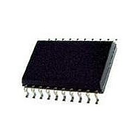
ATA5760N-TGQY Atmel, ATA5760N-TGQY Datasheet - Page 22

ATA5760N-TGQY
Manufacturer Part Number
ATA5760N-TGQY
Description
RF Receiver ASK/FSK Receiver 868 MHz
Manufacturer
Atmel
Type
UHF ASK/FSK Receiversr
Datasheet
1.ATA5760N-TGSY.pdf
(41 pages)
Specifications of ATA5760N-TGQY
Package / Case
SOIC-20
Operating Frequency
928 MHz
Operating Supply Voltage
5 V
Maximum Operating Temperature
+ 105 C
Minimum Operating Temperature
- 40 C
Mounting Style
SMD/SMT
Operating Temperature (min)
-40C
Operating Temperature (max)
105C
Operating Temperature Classification
Industrial
Operating Supply Voltage (min)
4.5V
Operating Supply Voltage (typ)
5V
Operating Supply Voltage (max)
5.5V
Lead Free Status / RoHS Status
Lead free / RoHS Compliant
Figure 10-2. Automatic Noise Suppression
Figure 10-3. Occurrence of a Pulse at the End of the Data Stream
10.2
Figure 10-4. Controlled Noise Suppression
22
Controlled Noise Suppression by the Microcontroller
(DATA_CLK)
POLLING/_ON
Serial bi-directional
data line
ATA5760/ATA5761
DATA_CLK
Data_out (DATA)
Dem_out
Data_out (DATA)
DATA_CLK
Bit-check
mode
Bit-check
mode
Bit check ok
Bit check ok
If the bit Noise_Disable (see
noise appears at the end of a valid data stream. To suppress the noise, the pin POLLING/_ON
must be set to Low. The receiver remains in receiving mode. Then, the OFF command causes
the change to the start-up mode. The programmed sleep time (see
not be executed because the level at pin POLLING/_ON is low, but the bit check is active in that
case. The OFF command activates the bit check also if the pin POLLING/_ON is held to Low.
The receiver changes back to receiving mode if the bit check was successful. To activate the
polling mode at the end of the data transmission, the pin POLLING/_ON must be set to High.
This way of suppressing the noise is recommended if the data stream is not Manchester or
Bi-phase coded.
Preburst
Preburst
Receiving mode,
data clock control
logic active
'1'
Receiving mode,
data clock control
logic active
Data stream
Data
Receiving mode
Timing error
Data
'1'
Digital Noise
'1'
t
OFF-command
ee
< T
T
Lim_min
Table 11-9 on page
ee
Bit-check
mode
OR T
Start-up
mode
Lim_max
T
Pulse
Bit-check
< t
mode
Bit check ok
ee
Bit check ok
< T
Digital noise
Lim_min_2T
25) in the OPMODE register is set to 0, digital
Preburst
Bit-check mode
Preburst
Receiving mode,
data clock control
logic active
OR t
ee
Receiving mode
> T
Data
Lim_max2T
Data
Table 11-7 on page
Digital Noise
Bit-check
mode
4896D–RKE–08/08
Sleep
mode
25) will


