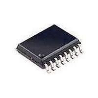
TDA1072ATD-T NXP Semiconductors, TDA1072ATD-T Datasheet - Page 4

TDA1072ATD-T
Manufacturer Part Number
TDA1072ATD-T
Description
RF Receiver AM RECEIVER CIRCUIT
Manufacturer
NXP Semiconductors
Type
Receiverr
Specifications of TDA1072ATD-T
Package / Case
SOT-109
Operating Supply Voltage
8.5 V
Maximum Operating Temperature
+ 80 C
Minimum Operating Temperature
- 40 C
Mounting Style
SMD/SMT
Operating Temperature (min)
-40C
Operating Temperature Classification
Commercial
Product Depth (mm)
4mm
Lead Free Status / RoHS Status
Lead free / RoHS Compliant
Other names
TDA1072AT/V4,118
Philips Semiconductors
Product specification
AM receiver circuit
TDA1072A
FUNCTIONAL DESCRIPTION
Gain-controlled r.f. stage and mixer
The differential amplifier in the r.f. stage employs an a.g.c. negative feedback network to provide a wide dynamic range.
Very good cross-modulation behaviour is achieved by a.g.c. delays at the various signal stages. Large signals are
handled with low distortion and the S/N ratio of small signals is improved. Low noise working is achieved in the differential
amplifier by using transistors with low base resistance.
A double balanced mixer provides the i.f. output signal to pin 1.
Oscillator
The differential amplifier oscillator is temperature compensated and is suitable for simple coil connection. The oscillator
is voltage-controlled and has little distortion or spurious radiation. It is specially suitable for electronic tuning using
variable capacitance diodes. Band switching diodes can easily be applied using the stabilized voltage V
. An extra
11-16
buffered oscillator output (pin 10) is available for driving a synthesizer. If this is not needed, resistor R
can be omitted.
L(10)
Gain-controlled i.f. amplifier
This amplifier comprises two cascaded, variable-gain differential amplifier stages coupled by a band-pass filter. Both
stages are gain-controlled by the a.g.c. negative feedback network.
Detector
The full-wave, balanced envelope detector has very low distortion over a wide dynamic range. Residual i.f. carrier is
blocked from the signal path by an internal low-pass filter.
A.F. preamplifier
This stage preamplifies the audio frequency output signal. The amplifier output has an emitter follower with a series
resistor which, together with an external capacitor, yields the required low-pass for a.f. filtering.
A.G.C. amplifier
The a.g.c. amplifier provides a control voltage which is proportional to the carrier amplitude. Second-order filtering of the
a.g.c. voltage achieves signals with very little distortion, even at low audio frequencies. This method of filtering also gives
fast a.g.c. settling time which is advantageous for electronic search tuning. The a.g.c. settling time can be further reduced
by using capacitors of smaller value in the external filter (C16 and C17). The a.g.c. voltage is fed to the r.f. and i.f. stages
via suitable a.g.c. delays. The capacitor at pin 7 can be omitted for low-cost applications.
Field strength indicator output
A buffered voltage source provides a high-level field strength output signal which has good linearity for logarithmic input
signals over the whole dynamic range. If the field strength information is not needed, R
can be omitted.
L(9)
Standby switch
This switch is primarily intended for AM/FM band switching. During standby mode the oscillator, mixer and a.f.
preamplifier are switched off.
Short-circuit protection
All pins have short-circuit protection to ground.
May 1984
4


