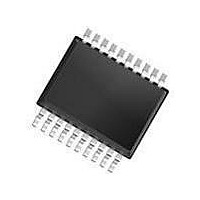
SA620DK-T NXP Semiconductors, SA620DK-T Datasheet - Page 2

SA620DK-T
Manufacturer Part Number
SA620DK-T
Description
Up-Down Converters 1 GHZ LV LNA MIXER AND VCO
Manufacturer
NXP Semiconductors
Datasheet
1.SA620DK118.pdf
(15 pages)
Specifications of SA620DK-T
Maximum Input Frequency
1200 MHz
Maximum Power Dissipation
980 mW
Mounting Style
SMD/SMT
Maximum Power Gain
4.5 dB
Operating Supply Voltage
3.3 V, 5 V
Maximum Operating Temperature
+ 85 C
Minimum Operating Temperature
- 40 C
Package / Case
SSOP-20
Operating Temperature (min)
-40C
Operating Temperature (max)
85C
Operating Temperature Classification
Industrial
Lead Free Status / RoHS Status
Lead free / RoHS Compliant
Other names
SA620DK,118
Philips Semiconductors
DESCRIPTION
The SA620 is a combined RF amplifier, VCO with tracking bandpass
filter and mixer designed for high-performance low-power
communication systems from 800-1200MHz. The low-noise
preamplifier has a 1.6dB noise figure at 900MHz with 11.5dB gain
and an IP3 intercept of -3dBm at the input. The gain is stabilized by
on-chip compensation to vary less than 0.2dB over -40 to +85 C
temperature range. The wide-dynamic-range mixer has an 9dB
noise figure and IP3 of –6dBm at the input at 900MHz. An external
LO can be used in place of the internal VCO for improved mixer
input IP3 and a 3mA reduction in current. The chip incorporates a
through-mode option so the RF amplifier can be disabled and
replaced by an attenuator (S
improving the overall dynamic range of the receiver when in an
overload situation. The nominal current drawn from a single 3V
supply is 10.4mA and 7.2mA in the thru-mode. Additionally, the
VCO and Mixer can be powered down to further reduce the supply
current to 1.2mA.
FEATURES
ORDERING INFORMATION
BLOCK DIAGRAM
2004 Dec 14
20-Pin Plastic Shrink Small Outline Package (Surface-mount, SSOP)
Low current consumption: 10.4mA nominal, 7.2mA with thru-mode
activated
Outstanding noise figure: 1.6dB for the amplifier and 9dB for the
mixer at 900MHz
Excellent gain stability versus temperature and supply voltage
Switchable overload capability
Independent LNA, mixer and VCO power down capability
Internal VCO automatic leveling loop
Monotonic VCO frequency vs control voltage
1GHz low voltage LNA, mixer and VCO
ENABLE
LNA
V
20
1
CC
21
= –7.5dB). This is useful for
DESCRIPTION
GND
19
GND
LNA
LNA
2
LNA IN
LNA
LNA
OUT
18
3
BIAS
17
LNA
GND
LNA
4
AUTOMATIC
LEVELING
Figure 2. Block Diagram
LOOP
MIXER
16
GND
LNA
IN
5
RF
MIXER
2
GND
OSC
GND
15
6
PIN CONFIGURATION
APPLICATIONS
LO
900MHz cellular front-end
900MHz cordless front-end
Spread spectrum receivers
RF data links
UHF frequency conversion
Portable radio
BYPASS
PWRDN
MIXER
MIXER
14
TEMPERATURE RANGE
7
IF
BANDPASS
TRACKING
FILTER
-40 to +85 C
MIXER PWRDN
PWRDN
MIXER
LNA ENABLE
OSC PWRDN
OUT
OSC
13
8
OSC GND
LNA GND
LNA GND
LNA GND
Figure 1. Pin Configuration
LNA IN
OSC1
OSC2
OSC1
OSC
GND
12
9
10
1
2
3
4
5
6
7
8
9
VCO
DK Package
OSC2
VCO
OUT
11
10
SR00115
ORDER CODE
SA620DK
20
19
18
17
16
15
14
13
12
11
V
LNA GND
LNA OUT
LNA BIAS
MIXER IN
MIXER GND
MIXER BYPASS
MIXER OUT
OSC GND
VCO OUT
CC
SR00114
SA620
Product data
SOT266-1
DWG #


