PCK953BD NXP Semiconductors, PCK953BD Datasheet
PCK953BD
Specifications of PCK953BD
Available stocks


Related parts for PCK953BD


PCK953BD Summary of contents
Page 1
PCK953 20 MHz to 125 MHz PECL input, 9 CMOS output, 3.3 V PLL clock driver Rev. 05 — 9 October 2008 1. General description The PCK953 is a 3.3 V compatible, PLL-based clock driver device targeted for high performance ...
Page 2
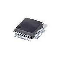
... MHz V 1 CCA 2 FB_CLK n. n.c. 6 n.c. GNDI 7 PECL_CLK 8 Pin configuration for LQFP32 Rev. 05 — 9 October 2008 7 1 CCO 22 Q2 PCK953BD 21 GNDO PCK953BD CCO GNDO 002aae137 © NXP B.V. 2008. All rights reserved. PCK953 Version SOT358-1 QFB 002aae138 ...
Page 3
... NXP Semiconductors 5.2 Pin description Table 2. Symbol V CCA FB_CLK n.c. GNDI PECL_CLK PECL_CLK MR/OE V CCO GNDO QFB PLL_EN BYPASS VCO_SEL 6. Functional description Refer to 6.1 Function selection Table 3. Pin BYPASS MR/OE VCO_SEL PLL_EN PCK953_5 Product data sheet 20 MHz to 125 MHz PECL input, 9 CMOS output, 3.3 V PLL clock driver ...
Page 4
... NXP Semiconductors 7. Limiting values Table 4. In accordance with the Absolute Maximum Rating System (IEC 60134). Symbol stg 8. Static characteristics Table 5. Static characteristics 3.3 V amb CC Symbol Parameter V HIGH-level input voltage IH V LOW-level input voltage IL V peak-to-peak input voltage i(p-p) V common-mode voltage cm V HIGH-level output voltage ...
Page 5
... NXP Semiconductors 9. Dynamic characteristics Table 6. Dynamic characteristics 3.3 V amb CC Symbol Parameter t output rise time r(o) t output fall time f(o) output duty cycle o t output skew time sk(o) f PLL VCO lock range VCO f maximum output frequency o(max) t (lock) input to EXT_FB delay (with ...
Page 6
... NXP Semiconductors 11. Application information 11.1 Power supply filtering The PCK953 is a mixed analog/digital product and as such it exhibits some sensitivities that would not necessarily be seen on a fully digital product. Analog circuitry is naturally susceptible to random noise, especially if this noise is seen on the power supply pins. The ...
Page 7
... NXP Semiconductors 11.2 Driving transmission lines The PCK953 clock driver was designed to drive high speed signals in a terminated transmission line environment. To provide the optimum flexibility to the user, the output drivers were designed to exhibit the lowest impedance possible. With an output impedance of less than 20 , the drivers can drive either parallel or series terminated transmission lines ...
Page 8
... NXP Semiconductors the load end, the voltage will double due to the near unity reflection coefficient will then increment towards the quiescent 3 steps separated by one round-trip delay (in this case, 4.0 ns). Fig 5. Since this step is well above the threshold region, it will not cause any false clock triggering, however, designers may be uncomfortable with unwanted refl ...
Page 9
... NXP Semiconductors 12. Package outline LQFP32: plastic low profile quad flat package; 32 leads; body 1 pin 1 index DIMENSIONS (mm are the original dimensions) A UNIT max. 0.20 1.45 mm 1.6 0.25 0.05 1.35 Note 1. Plastic or metal protrusions of 0.25 mm maximum per side are not included. OUTLINE VERSION ...
Page 10
... PCK953BD 9352 679 41151 PCK953BD 9352 679 41157 PCK953BD/G 9352 761 22128 14. Soldering of SMD packages This text provides a very brief insight into a complex technology. A more in-depth account of soldering ICs can be found in Application Note AN10365 “Surface mount reflow soldering description” . ...
Page 11
... NXP Semiconductors • Package footprints, including solder thieves and orientation • The moisture sensitivity level of the packages • Package placement • Inspection and repair • Lead-free soldering versus SnPb soldering 14.3 Wave soldering Key characteristics in wave soldering are: • Process issues, such as application of adhesive and flux, clinching of leads, board ...
Page 12
... NXP Semiconductors Studies have shown that small packages reach higher temperatures during reflow soldering, see Fig 8. For further information on temperature profiles, refer to Application Note AN10365 “Surface mount reflow soldering description” . 15. Abbreviations Table 11. Acronym CMOS LPF LVCMOS LVPECL LVTTL PECL ...
Page 13
... NXP Semiconductors. • Legal texts have been adapted to the new company name where appropriate. • Section 2 • Section 3 “Ordering – added Type number PCK953BD/G – added paragraph following • Table 4 “Limiting “Disclaimers”) • Table 5 “Static – changed title of this table from “DC characteristics” to “Static characteristics” ...
Page 14
... Right to make changes — NXP Semiconductors reserves the right to make changes to information published in this document, including without limitation specifications and product descriptions, at any time and without notice ...
Page 15
... NXP Semiconductors 19. Contents 1 General description . . . . . . . . . . . . . . . . . . . . . . 1 2 Features . . . . . . . . . . . . . . . . . . . . . . . . . . . . . . . 1 3 Ordering information . . . . . . . . . . . . . . . . . . . . . 2 4 Functional diagram . . . . . . . . . . . . . . . . . . . . . . 2 5 Pinning information . . . . . . . . . . . . . . . . . . . . . . 2 5.1 Pinning . . . . . . . . . . . . . . . . . . . . . . . . . . . . . . . 2 5.2 Pin description . . . . . . . . . . . . . . . . . . . . . . . . . 3 6 Functional description . . . . . . . . . . . . . . . . . . . 3 6.1 Function selection Limiting values Static characteristics Dynamic characteristics . . . . . . . . . . . . . . . . . . 5 10 PLL input reference characteristics Application information 11.1 Power supply fi ...