BC849CW,115 NXP Semiconductors, BC849CW,115 Datasheet - Page 2
BC849CW,115
Manufacturer Part Number
BC849CW,115
Description
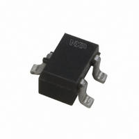
TRANSISTOR NPN 30V 100MA SOT323
Manufacturer
NXP Semiconductors
Datasheet
1.BC849CW115.pdf
(7 pages)
Specifications of BC849CW,115
Package / Case
SC-70-3, SOT-323-3
Mounting Type
Surface Mount
Power - Max
200mW
Current - Collector (ic) (max)
100mA
Voltage - Collector Emitter Breakdown (max)
30V
Transistor Type
NPN
Frequency - Transition
100MHz
Dc Current Gain (hfe) (min) @ Ic, Vce
420 @ 2mA, 5V
Vce Saturation (max) @ Ib, Ic
600mV @ 5mA, 100mA
Dc Collector/base Gain Hfe Min
420
Minimum Operating Temperature
- 65 C
Configuration
Single
Transistor Polarity
NPN
Mounting Style
SMD/SMT
Collector- Emitter Voltage Vceo Max
30 V
Emitter- Base Voltage Vebo
5 V
Continuous Collector Current
100 mA
Maximum Dc Collector Current
200 mA
Power Dissipation
200 mW
Maximum Operating Frequency
100 MHz
Maximum Operating Temperature
+ 150 C
Lead Free Status / RoHS Status
Lead free / RoHS Compliant
Current - Collector Cutoff (max)
-
Lead Free Status / Rohs Status
Lead free / RoHS Compliant
Other names
934022070115::BC849CW T/R::BC849CW T/R
Available stocks
Company
Part Number
Manufacturer
Quantity
Price
Company:

Part Number:
BC849CW,115
Manufacturer:
NXP Semiconductors
Quantity:
12 800


NXP Semiconductors
FEATURES
• Low current (max. 100 mA)
• Low voltage (max. 45 V).
APPLICATIONS
• Low noise stages in tape recorders, hi-fi amplifiers and
DESCRIPTION
NPN transistor in a SOT323 plastic package.
PNP complements: BC859W and BC860W.
MARKING
Note
1. ∗ = - : Made in Hong Kong.
LIMITING VALUES
In accordance with the Absolute Maximum Rating System (IEC 134).
Note
1. Transistor mounted on an FR4 printed-circuit board.
1999 Apr 12
BC849BW
BC849CW
V
V
V
I
I
I
P
T
T
T
C
CM
BM
SYMBOL
other audio-frequency equipment.
NUMBER
stg
j
amb
CBO
CEO
EBO
tot
NPN general purpose transistors
∗ = t : Made in Malaysia.
TYPE
collector-base voltage
collector-emitter voltage
emitter-base voltage
collector current (DC)
peak collector current
peak base current
total power dissipation
storage temperature
junction temperature
operating ambient temperature
MARKING
BC849W
BC850W
BC849W
BC850W
CODE
2B∗
2C∗
(1)
PARAMETER
BC850BW
BC850CW
NUMBER
TYPE
MARKING
CODE
2G∗
2F∗
open emitter
open base
open collector
T
(1)
amb
≤ 25 °C; note 1
2
CONDITIONS
PINNING
handbook, halfpage
Fig.1
PIN
1
2
3
Simplified outline (SOT323) and symbol.
Top view
base
emitter
collector
1
3
−
−
−
−
−
−
−
−
−
−65
−
−65
BC849W; BC850W
MIN.
DESCRIPTION
2
MAM062
30
50
30
45
5
100
200
200
200
+150
150
+150
Product data sheet
MAX.
1
3
2
V
V
V
V
V
mA
mA
mA
mW
°C
°C
°C
UNIT
Related parts for BC849CW,115
Image
Part Number
Description
Manufacturer
Datasheet
Request
R


Part Number:
Description:
TRANSISTOR NPN 30V 100MA SOT323
Manufacturer:
NXP Semiconductors
Datasheet:

Part Number:
Description:
Transistors Bipolar - BJT TRANS LOW NOISE TAPE-11
Manufacturer:
NXP Semiconductors
Datasheet:
Part Number:
Description:
Transistors Bipolar - BJT TRANS LOW NOISE TAPE-7
Manufacturer:
NXP Semiconductors
Datasheet:

Part Number:
Description:
TRANSISTOR NPN 30V 100MA SOT23
Manufacturer:
NXP Semiconductors
Datasheet:
Part Number:
Description:
TRANSISTOR NPN 30V 100MA SOT23
Manufacturer:
NXP Semiconductors
Datasheet:
Part Number:
Description:
Transistors Bipolar - BJT TRANS LOW NOISE TAPE-11
Manufacturer:
NXP Semiconductors
Datasheet:
Part Number:
Description:
NXP Semiconductors designed the LPC2420/2460 microcontroller around a 16-bit/32-bitARM7TDMI-S CPU core with real-time debug interfaces that include both JTAG andembedded trace
Manufacturer:
NXP Semiconductors
Datasheet:

Part Number:
Description:
NXP Semiconductors designed the LPC2458 microcontroller around a 16-bit/32-bitARM7TDMI-S CPU core with real-time debug interfaces that include both JTAG andembedded trace
Manufacturer:
NXP Semiconductors
Datasheet:
Part Number:
Description:
NXP Semiconductors designed the LPC2468 microcontroller around a 16-bit/32-bitARM7TDMI-S CPU core with real-time debug interfaces that include both JTAG andembedded trace
Manufacturer:
NXP Semiconductors
Datasheet:
Part Number:
Description:
NXP Semiconductors designed the LPC2470 microcontroller, powered by theARM7TDMI-S core, to be a highly integrated microcontroller for a wide range ofapplications that require advanced communications and high quality graphic displays
Manufacturer:
NXP Semiconductors
Datasheet:
Part Number:
Description:
NXP Semiconductors designed the LPC2478 microcontroller, powered by theARM7TDMI-S core, to be a highly integrated microcontroller for a wide range ofapplications that require advanced communications and high quality graphic displays
Manufacturer:
NXP Semiconductors
Datasheet:
Part Number:
Description:
The Philips Semiconductors XA (eXtended Architecture) family of 16-bit single-chip microcontrollers is powerful enough to easily handle the requirements of high performance embedded applications, yet inexpensive enough to compete in the market for hi
Manufacturer:
NXP Semiconductors
Datasheet:
Part Number:
Description:
The XA-S3 device is a member of Philips Semiconductors? XA(eXtended Architecture) family of high performance 16-bitsingle-chip microcontrollers
Manufacturer:
NXP Semiconductors
Datasheet: