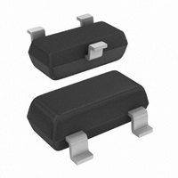
BFS20,215 NXP Semiconductors, BFS20,215 Datasheet - Page 2

BFS20,215
Manufacturer Part Number
BFS20,215
Description
TRANS NPN 20V 25MA SOT233
Manufacturer
NXP Semiconductors
Series
-r
Datasheet
1.BFS20235.pdf
(6 pages)
Specifications of BFS20,215
Package / Case
SOT-23-3, TO-236-3, Micro3™, SSD3, SST3
Transistor Type
NPN
Current - Collector (ic) (max)
25mA
Voltage - Collector Emitter Breakdown (max)
20V
Dc Current Gain (hfe) (min) @ Ic, Vce
40 @ 7mA, 10V
Power - Max
250mW
Frequency - Transition
450MHz
Mounting Type
Surface Mount
Dc Collector/base Gain Hfe Min
40
Dc Current Gain Hfe Max
40 @ 7mA @ 10V
Minimum Operating Temperature
- 65 C
Mounting Style
SMD/SMT
Configuration
Single
Transistor Polarity
NPN
Maximum Operating Frequency
450 MHz (Typ)
Collector- Emitter Voltage Vceo Max
20 V
Emitter- Base Voltage Vebo
4 V
Continuous Collector Current
25 mA
Power Dissipation
250 mW
Maximum Operating Temperature
+ 150 C
Vce Saturation (max) @ Ib, Ic
-
Current - Collector Cutoff (max)
-
Lead Free Status / RoHS Status
Lead free / RoHS Compliant
Current - Collector Cutoff (max)
-
Vce Saturation (max) @ Ib, Ic
-
Lead Free Status / Rohs Status
Lead free / RoHS Compliant
Other names
933092111215
BFS20 T/R
BFS20 T/R
BFS20 T/R
BFS20 T/R
Available stocks
Company
Part Number
Manufacturer
Quantity
Price
Part Number:
BFS20,215
Manufacturer:
NEXPERIA/安世
Quantity:
20 000
NXP Semiconductors
FEATURES
• I
• V
• Very low feedback capacitance (typ. 350 fF).
APPLICATIONS
• IF and VHF thick and thin-film circuit applications.
DESCRIPTION
NPN medium frequency transistor in a SOT23 plastic
package.
MARKING
Note
1. * = p : Made in Hong Kong.
ORDERING INFORMATION
LIMITING VALUES
In accordance with the Absolute Maximum Rating System (IEC 60134).
Note
1. Transistor mounted on an FR4 printed-circuit board.
2004 Feb 05
BFS20
BFS20
V
V
V
I
I
P
T
T
T
NUMBER
SYMBOL
C
CM
stg
j
amb
CBO
CEO
EBO
tot
NPN medium frequency transistor
C(max)
TYPE
CEO(max)
* = t : Made in Malaysia.
* = W : Made in China.
TYPE NUMBER
= 25 mA
= 20 V
collector-base voltage
collector-emitter voltage
emitter-base voltage
collector current (DC)
peak collector current
total power dissipation
storage temperature
junction temperature
operating ambient temperature
NAME
−
PARAMETER
MARKING CODE
plastic surface mounted package; 3 leads
G1*
open emitter
open base
open collector
T
(1)
amb
≤ 25 °C; note 1
DESCRIPTION
2
CONDITIONS
PACKAGE
PINNING
handbook, halfpage
Fig.1 Simplified outline (SOT23) and symbol.
Top view
PIN
1
2
3
1
3
base
emitter
collector
−
−
−
−
−
−
−65
−
−65
MIN.
2
DESCRIPTION
MAM255
30
20
4
25
25
250
+150
150
+150
MAX.
Product data sheet
1
VERSION
SOT23
BFS20
3
2
V
V
V
mA
mA
mW
°C
°C
°C
UNIT


