BUV22G ON Semiconductor, BUV22G Datasheet
BUV22G
Specifications of BUV22G


Related parts for BUV22G


BUV22G Summary of contents
Page 1
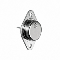
... JC BUV22 BUV22G 1 http://onsemi.com 40 AMPERES NPN SILICON POWER METAL TRANSISTOR 250 VOLTS − 250 WATTS TO−204AE (TO−3) CASE 197A MARKING DIAGRAM BUV22G AYWW MEX BUV22 = Device Code G = Pb−Free Package A = Assembly Location Y = Year WW = Work Week MEX = Country of Origin ORDERING INFORMATION ...
Page 2
ELECTRICAL CHARACTERISTICS Î Î Î Î Î ...
Page 3
V , COLLECTOR−EMITTER VOLTAGE (V) CE Figure 2. Active Region Safe Operating Area 2 1.6 1.2 0.8 0 COLLECTOR CURRENT (A) C Figure ...
Page 4
... American Technical Support: 800−282−9855 Toll Free USA/Canada Japan: ON Semiconductor, Japan Customer Focus Center 2−9−1 Kamimeguro, Meguro−ku, Tokyo, Japan 153−0051 Phone: 81−3−5773−3850 http://onsemi.com 4 NOTES: 1. DIMENSIONING AND TOLERANCING PER ANSI Y14.5M, 1982. 2. CONTROLLING DIMENSION: INCH. ...