MJD117T4 ON Semiconductor, MJD117T4 Datasheet
MJD117T4
Specifications of MJD117T4
Available stocks


Related parts for MJD117T4


MJD117T4 Summary of contents
Page 1
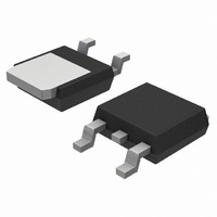
MJD112 (NPN) MJD117 (PNP) Complementary Darlington Power Transistors DPAK For Surface Mount Applications Designed for general purpose power and switching such as output or driver stages in applications such as switching regulators, converters, and power amplifiers. Features • Lead Formed ...
Page 2
ELECTRICAL CHARACTERISTICS Î Î Î Î Î ...
Page 3
D = 0.5 0.5 0.3 0.2 0.2 0.1 0.05 0.1 0.07 0.01 0.05 0.03 SINGLE PULSE 0.02 0.01 0.01 0.02 0.03 0.05 0 0.7 0.5 dc 0.3 0.2 ...
Page 4
TYPICAL ELECTRICAL CHARACTERISTICS NPN MJD112 125° 25° 800 - 55°C 600 400 300 0.04 0.06 0.1 0.2 0.4 0 COLLECTOR CURRENT (AMP) C 3.4 3 ...
Page 5
NPN MJD112 + 0.8 *APPLIED FOR I /I < 0.8 25°C TO 150°C - 1.6 *q FOR V - 2.4 VC CE(sat) - 55°C TO 25°C - 3.2 25°C TO 150°C q FOR ...
Page 6
... MJD112RL MJD112RLG MJD112T4 MJD112T4G MJD117 MJD117G MJD117−001 MJD117−1G MJD117T4 MJD117T4G †For information on tape and reel specifications, including part orientation and tape sizes, please refer to our Tape and Reel Packaging Specifications Brochure, BRD8011/D. Package Type Package DPAK 369C DPAK (Pb−Free) DPAK− ...
Page 7
... DETAIL 0.005 (0.13 5.80 0.228 *For additional information on our Pb−Free strategy and soldering details, please download the ON Semiconductor Soldering and Mounting Techniques Reference Manual, SOLDERRM/D. PACKAGE DIMENSIONS DPAK CASE 369C−01 ISSUE GAUGE SEATING L2 C PLANE PLANE DETAIL A ROTATED SOLDERING FOOTPRINT* 6 ...
Page 8
... Opportunity/Affirmative Action Employer. This literature is subject to all applicable copyright laws and is not for resale in any manner. PUBLICATION ORDERING INFORMATION LITERATURE FULFILLMENT: Literature Distribution Center for ON Semiconductor P.O. Box 5163, Denver, Colorado 80217 USA Phone: 303−675−2175 or 800−344−3860 Toll Free USA/Canada Fax: 303− ...