MJD117T4 ON Semiconductor, MJD117T4 Datasheet - Page 7
MJD117T4
Manufacturer Part Number
MJD117T4
Description
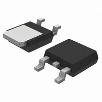
TRANS DARL PNP 2A 100V DPAK
Manufacturer
ON Semiconductor
Datasheet
1.MJD117T4G.pdf
(8 pages)
Specifications of MJD117T4
Transistor Type
PNP - Darlington
Current - Collector (ic) (max)
2A
Voltage - Collector Emitter Breakdown (max)
100V
Vce Saturation (max) @ Ib, Ic
3V @ 40mA, 4A
Current - Collector Cutoff (max)
20µA
Dc Current Gain (hfe) (min) @ Ic, Vce
1000 @ 2A, 3V
Power - Max
1.75W
Frequency - Transition
25MHz
Mounting Type
Surface Mount
Package / Case
DPak, TO-252 (2 leads+tab), SC-63
Lead Free Status / RoHS Status
Contains lead / RoHS non-compliant
Other names
MJD117T4OSCT
Available stocks
Company
Part Number
Manufacturer
Quantity
Price

Company:
Part Number:
MJD117T4G
Manufacturer:
ON
Quantity:
12 500
Part Number:
MJD117T4G
Manufacturer:
ON/安森美
Quantity:
20 000


L3
L4
b2
e
1
b3
4
2
E
3
b
A
D
0.005 (0.13)
B
*For additional information on our Pb−Free strategy and soldering
details, please download the ON Semiconductor Soldering and
Mounting Techniques Reference Manual, SOLDERRM/D.
M
DETAIL A
0.228
C
5.80
c
L2
A
GAUGE
PLANE
PACKAGE DIMENSIONS
SOLDERING FOOTPRINT*
ROTATED 90 CW
0.244
0.101
6.20
c2
2.58
DETAIL A
H
C
http://onsemi.com
L
CASE 369C−01
L1
ISSUE D
DPAK
5
7
A1
0.118
3.0
H
0.063
1.6
SCALE 3:1
C
Z
SEATING
PLANE
6.172
0.243
inches
NOTES:
mm
1. DIMENSIONING AND TOLERANCING PER ASME
2. CONTROLLING DIMENSION: INCHES.
3. THERMAL PAD CONTOUR OPTIONAL WITHIN DI-
4. DIMENSIONS D AND E DO NOT INCLUDE MOLD
5. DIMENSIONS D AND E ARE DETERMINED AT THE
6. DATUMS A AND B ARE DETERMINED AT DATUM
Y14.5M, 1994.
MENSIONS b3, L3 and Z.
FLASH, PROTRUSIONS, OR BURRS. MOLD
FLASH, PROTRUSIONS, OR GATE BURRS SHALL
NOT EXCEED 0.006 INCHES PER SIDE.
OUTERMOST EXTREMES OF THE PLASTIC BODY.
PLANE H.
STYLE 1:
DIM
A1
b2
b3
c2
L1
L2
L3
L4
PIN 1. BASE
A
b
D
E
H
L
Z
c
e
2. COLLECTOR
3. EMITTER
4. COLLECTOR
0.086
0.000
0.025
0.030
0.180
0.018
0.018
0.235
0.250
0.370
0.055
0.035
0.155
MIN
−−−
0.090 BSC
0.108 REF
0.020 BSC
INCHES
0.094
0.005
0.035
0.045
0.215
0.024
0.024
0.245
0.265
0.410
0.070
0.050
0.040
MAX
−−−
MILLIMETERS
2.18
0.00
0.63
0.76
4.57
0.46
0.46
5.97
6.35
9.40
1.40
0.89
3.93
MIN
−−−
2.29 BSC
2.74 REF
0.51 BSC
10.41
MAX
2.38
0.13
0.89
1.14
5.46
0.61
0.61
6.22
6.73
1.78
1.27
1.01
−−−
Related parts for MJD117T4
Image
Part Number
Description
Manufacturer
Datasheet
Request
R

Part Number:
Description:
TRANS DARL PNP 2A 100V DPAK-3
Manufacturer:
ON Semiconductor
Datasheet:

Part Number:
Description:
TRANS DARL PNP 2A 100V DPAK
Manufacturer:
ON Semiconductor
Datasheet:
Part Number:
Description:
TRANS DARL PNP 2A 100V DPAK-3
Manufacturer:
ON Semiconductor
Datasheet:

Part Number:
Description:
ON Semiconductor [VOLTAGE REGULATOR]
Manufacturer:
ON Semiconductor
Datasheet:
Part Number:
Description:
357-036-542-201 CARDEDGE 36POS DL .156 BLK LOPRO
Manufacturer:
ON Semiconductor
Datasheet:
Part Number:
Description:
357-036-542-201 CARDEDGE 36POS DL .156 BLK LOPRO
Manufacturer:
ON Semiconductor
Datasheet:
Part Number:
Description:
357-036-542-201 CARDEDGE 36POS DL .156 BLK LOPRO
Manufacturer:
ON Semiconductor
Datasheet:
Part Number:
Description:
357-036-542-201 CARDEDGE 36POS DL .156 BLK LOPRO
Manufacturer:
ON Semiconductor
Datasheet:
Part Number:
Description:
357-036-542-201 CARDEDGE 36POS DL .156 BLK LOPRO
Manufacturer:
ON Semiconductor
Datasheet:
Part Number:
Description:
357-036-542-201 CARDEDGE 36POS DL .156 BLK LOPRO
Manufacturer:
ON Semiconductor
Datasheet:
Part Number:
Description:
357-036-542-201 CARDEDGE 36POS DL .156 BLK LOPRO
Manufacturer:
ON Semiconductor
Datasheet:
Part Number:
Description:
357-036-542-201 CARDEDGE 36POS DL .156 BLK LOPRO
Manufacturer:
ON Semiconductor
Datasheet:
Part Number:
Description:
357-036-542-201 CARDEDGE 36POS DL .156 BLK LOPRO
Manufacturer:
ON Semiconductor
Datasheet:
Part Number:
Description:
357-036-542-201 CARDEDGE 36POS DL .156 BLK LOPRO
Manufacturer:
ON Semiconductor
Datasheet: