BT1308-400D,412 NXP Semiconductors, BT1308-400D,412 Datasheet
BT1308-400D,412
Specifications of BT1308-400D,412
BT1308-400D
BT1308-400D


Related parts for BT1308-400D,412


BT1308-400D,412 Summary of contents
Page 1
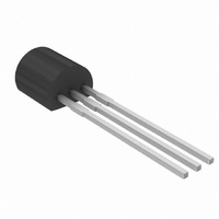
... DRM I I TSM 2. Pinning information Table 1. Pinning Pin Description 1 main terminal 2 (T2) 2 gate (G) 3 main terminal 1 (T1) 400 V (BT1308-400D) 600 V (BT1308-600D ms) Simplified outline Product data sheet I Gate triggering in four quadrants I Direct interfacing to low-power gate drive circuits I Low-power AC fan speed control ...
Page 2
... Conditions BT1308-400D BT1308-600D full sine wave; T see Figure 4 and see Figure 2 and 16 mA T2 over any 20 ms period Rev. 01 — 26 February 2008 BT1308 series D Min - - lead prior to surge / Triacs logic level Version SOT54 ...
Page 3
... Total power dissipation as a function of RMS on-state current; maximum values 12 I TSM ( Fig 2. Non-repetitive peak on-state current as a function of the number of sinusoidal current cycles; maximum values BT1308_SER_D_1 Product data sheet 0.4 0 Rev. 01 — 26 February 2008 BT1308 series D Triacs logic level 003aac209 = 180 120 0 (A) T(RMS) 003aac207 TSM t 1/f ...
Page 4
... lead Fig 4. RMS on-state current as a function of surge duration; maximum values BT1308_SER_D_1 Product data sheet - 003aaa617 I T(RMS) ( surge duration (s) Fig 5. Rev. 01 — 26 February 2008 BT1308 series max j(init 0.8 0.6 0.4 0 100 RMS on-state current as a function of lead temperature; maximum values © ...
Page 5
... Transient thermal impedance from junction to solder point as a function of pulse width BT1308_SER_D_1 Product data sheet Conditions full cycle full cycle; printed-circuit board mounted; lead length 4 mm; see Figure Rev. 01 — 26 February 2008 BT1308 series D Triacs logic level Min Typ Max - - 60 - 150 - 003aac206 P t ...
Page 6
... 0.1 A; see Figure 0 110 C D DRM 125 C D DRM(max 0. 110 C; DM DRM(max) j exponential waveform; gate open circuit DRM(max 0. /dt = 0.3 A/ms TM com mA DRM(max / Rev. 01 — 26 February 2008 BT1308 series D Triacs logic level Min Typ Max Unit - 1. 0.1 0 0.1 0.5 ...
Page 7
... BT1308_SER_D_1 Product data sheet 003aaa039 GT( 140 Fig 8. 003aab486 I L(25 C) (2) (3) 1.2 1 (V) T Fig 10. Normalized latching current as a function of Rev. 01 — 26 February 2008 BT1308 series D 3 (1) (2) 2 (3) (4) (1) (2) ( (1) T2 (4) T2+ G Normalized gate trigger current as a function of junction temperature ...
Page 8
... NXP Semiconductors Fig 11. Normalized holding current as a function of junction temperature BT1308_SER_D_1 Product data sheet 2 H(25 C) 1.5 1.0 0 Rev. 01 — 26 February 2008 BT1308 series D Triacs logic level 003aaa032 90 140 © NXP B.V. 2008. All rights reserved ...
Page 9
... 4.8 1.7 4.2 14.5 2.54 1.27 4.4 1.4 3.6 12.7 REFERENCES JEDEC JEITA TO-92 SC-43A Rev. 01 — 26 February 2008 BT1308 series D Triacs logic level ( max. 2.5 EUROPEAN ISSUE DATE PROJECTION © NXP B.V. 2008. All rights reserved. SOT54 04-06-28 04-11- ...
Page 10
... NXP Semiconductors 8. Revision history Table 6. Revision history Document ID Release date BT1308_SER_D_1 20080226 BT1308_SER_D_1 Product data sheet Data sheet status Change notice Product data sheet - Rev. 01 — 26 February 2008 BT1308 series D Triacs logic level Supersedes - © NXP B.V. 2008. All rights reserved ...
Page 11
... Notice: All referenced brands, product names, service names and trademarks are the property of their respective owners. http://www.nxp.com salesaddresses@nxp.com Rev. 01 — 26 February 2008 BT1308 series D Triacs logic level Trademarks © NXP B.V. 2008. All rights reserved ...
Page 12
... NXP B.V. 2008. For more information, please visit: http://www.nxp.com For sales office addresses, please send an email to: salesaddresses@nxp.com Document identifier: BT1308_SER_D_1 Triacs logic level All rights reserved. Date of release: 26 February 2008 ...