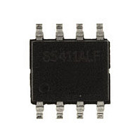
85411AMLF IDT, Integrated Device Technology Inc, 85411AMLF Datasheet

85411AMLF
Specifications of 85411AMLF
Related parts for 85411AMLF
85411AMLF Summary of contents
Page 1
LOW SKEW, 1-TO-2 DIFFERENTIAL-TO- LVDS FANOUT BUFFER G D ENERAL ESCRIPTION The ICS85411 is a low skew, high performance IC S 1-to-2 Differential-to-LVDS Fanout Buffer and a HiPerClockS™ member of the HiPerClock S™ family of High Performance Clock Solutions from ...
Page 2
ICS85411 LOW SKEW, 1-TO-2 DIFFERENTIAL-TO-LVDS FANOUT BUFFER ABLE IN ESCRIPTIONS ...
Page 3
ICS85411 LOW SKEW, 1-TO-2 DIFFERENTIAL-TO-LVDS FANOUT BUFFER BSOLUTE AXIMUM ATINGS Supply Voltage Inputs, V -0. Outputs Continuous Current 10mA Surge Current 15mA Package Thermal Impedance, JA Storage Temperature, T -65°C ...
Page 4
ICS85411 LOW SKEW, 1-TO-2 DIFFERENTIAL-TO-LVDS FANOUT BUFFER 3.3V±10% T ABLE HARACTERISTICS ...
Page 5
ICS85411 LOW SKEW, 1-TO-2 DIFFERENTIAL-TO-LVDS FANOUT BUFFER The spectral purity in a band at a specific offset from the fundamental compared to the power of the fundamental is called the dBc Phase Noise. This value is normally expressed using a ...
Page 6
ICS85411 LOW SKEW, 1-TO-2 DIFFERENTIAL-TO-LVDS FANOUT BUFFER P ARAMETER V 3.3V±10% DD POWER SUPPLY LVDS + Float GND – 3. UTPUT OAD EST IRCUIT nQx PART 1 Qx nQy PART 2 Qy tsk(pp ...
Page 7
ICS85411 LOW SKEW, 1-TO-2 DIFFERENTIAL-TO-LVDS FANOUT BUFFER P ARAMETER V DD LVDS DC Input ➤ FFSET OLTAGE ETUP V DD LVDS DC Input UTPUT HORT IRCUIT URRENT ETUP IDT ™ / ICS ...
Page 8
ICS85411 LOW SKEW, 1-TO-2 DIFFERENTIAL-TO-LVDS FANOUT BUFFER IRING THE IFFERENTIAL NPUT TO Figure 1 shows how the differential input can be wired to accept single ended levels. The reference voltage V_REF = V generated by the bias ...
Page 9
ICS85411 LOW SKEW, 1-TO-2 DIFFERENTIAL-TO-LVDS FANOUT BUFFER IFFERENTIAL LOCK NPUT NTERFACE The CLK /nCLK accepts LVDS, LVPECL, LVHSTL, SSTL, HCSL and other differential signals. Both signals must meet the V V input requirements. Figures 2A to ...
Page 10
ICS85411 LOW SKEW, 1-TO-2 DIFFERENTIAL-TO-LVDS FANOUT BUFFER LVDS D T RIVER ERMINATION A general LVDS interface is shown in Figure 100 differential transmission line environment, LVDS drivers require a matched load termination of 100 3.3V IDT ™ ...
Page 11
ICS85411 LOW SKEW, 1-TO-2 DIFFERENTIAL-TO-LVDS FANOUT BUFFER This section provides information on power dissipation and junction temperature for the ICS85411. Equations and example calculations are also provided. 1. Power Dissipation. The total power dissipation for the ICS85411 is the sum ...
Page 12
ICS85411 LOW SKEW, 1-TO-2 DIFFERENTIAL-TO-LVDS FANOUT BUFFER ABLE VS IR LOW ABLE FOR JA Single-Layer PCB, JEDEC Standard Test Boards Multi-Layer PCB, JEDEC Standard Test Boards NOTE: Most modern PCB designs use multi-layered boards. ...
Page 13
ICS85411 LOW SKEW, 1-TO-2 DIFFERENTIAL-TO-LVDS FANOUT BUFFER ABLE RDERING NFORMATION ...
Page 14
ICS85411 LOW SKEW, 1-TO-2 DIFFERENTIAL-TO-LVDS FANOUT BUFFER ...
Page 15
ICS85411 LOW SKEW, 1-TO-2 DIFFERENTIAL-TO-LVDS FANOUT BUFFER Innovate with IDT and accelerate your future networks. Contact: www.IDT.com For Sales 800-345-7015 (inside USA) +408-284-8200 (outside USA) Fax: 408-284-2775 www.IDT.com/go/contactIDT © 2009 Integrated Device Technology, Inc. All rights reserved. Product specifications subject ...


