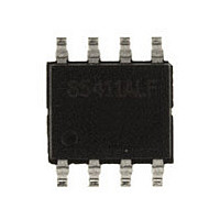
85411AMLF IDT, Integrated Device Technology Inc, 85411AMLF Datasheet - Page 8

85411AMLF
Manufacturer Part Number
85411AMLF
Description
Manufacturer
IDT, Integrated Device Technology Inc
Datasheet
1.85411AMLF.pdf
(15 pages)
Specifications of 85411AMLF
Number Of Outputs
4
Operating Supply Voltage (max)
3.63V
Operating Temp Range
0C to 70C
Propagation Delay Time
2.5ns
Operating Supply Voltage (min)
2.97V
Mounting
Surface Mount
Pin Count
8
Operating Supply Voltage (typ)
3.3V
Package Type
SOIC
Input Frequency
650MHz
Duty Cycle
53%
Operating Temperature Classification
Commercial
Lead Free Status / RoHS Status
Compliant
W
IDT
Figure 1 shows how the differential input can be wired to accept
single ended levels. The reference voltage V_REF = V
generated by the bias resistors R1, R2 and C1. This bias circuit
should be located as close as possible to the input pin. The ratio
R
O
LVDS
All unused LVDS output pairs can be either left floating or
terminated with 100
should be no trace attached.
ECOMMENDATIONS FOR
ICS85411
LOW SKEW, 1-TO-2 DIFFERENTIAL-TO-LVDS FANOUT BUFFER
UTPUTS
IRING THE
™
/ ICS
™
:
DIFFERENTIAL-TO-LVDS FANOUT BUFFER
D
IFFERENTIAL
across. If they are left floating, there
U
NUSED
I
NPUT TO
F
IGURE
O
Single Ended Clock Input
UTPUT
A
CCEPT
1. S
A
PPLICATION
P
INGLE
INS
S
INGLE
E
C1
0.1u
NDED
V_REF
DD
E
/2 is
S
NDED
IGNAL
8
I
L
NFORMATION
of R1 and R2 might need to be adjusted to position the V_REF in
the center of the input voltage swing. For example, if the input
clock swing is only 2.5V and V
and R2/R1 = 0.609.
1K
D
R1
1K
R2
EVELS
RIVING
VDD
CLK
nCLK
D
IFFERENTIAL
I
NPUT
ICS85411AM REV. C JANUARY 20, 2009
DD
= 3.3V, V_REF should be 1.25V


