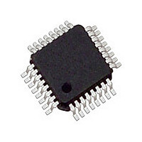
IDT5T93GL061PFI IDT, Integrated Device Technology Inc, IDT5T93GL061PFI Datasheet

IDT5T93GL061PFI
Specifications of IDT5T93GL061PFI
Related parts for IDT5T93GL061PFI
IDT5T93GL061PFI Summary of contents
Page 1
IDT5T93GL061 2.5V LVDS 1:6 GLITCHLESS CLOCK BUFFER TERABUFFER II FEATURES: • Guaranteed Low Skew < 50ps (max) • Very low duty cycle distortion < 100ps (max) • High speed propagation delay < 2.2ns (max) • 450MHz operation • ...
Page 2
IDT5T93GL061 2.5V LVDS 1:6 GLITCHLESS CLOCK BUFFER TERABUFFER II PIN CONFIGURATION GND GND ...
Page 3
IDT5T93GL061 2.5V LVDS 1:6 GLITCHLESS CLOCK BUFFER TERABUFFER II ABSOLUTE MAXIMUM RATINGS Symbol Description V Power Supply Voltage DD V Input Voltage I V Output Voltage ( Storage Temperature STG T Junction Temperature J NOTES: 1. Stresses greater ...
Page 4
IDT5T93GL061 2.5V LVDS 1:6 GLITCHLESS CLOCK BUFFER TERABUFFER II DC ELECTRICAL CHARACTERISTICS OVER RECOMMENDED OPERATING RANGE FOR LVTTL (1) Symbol Parameter Input Characteristics I Input HIGH Current IH I Input LOW Current IL V Clamp Diode Voltage ...
Page 5
IDT5T93GL061 2.5V LVDS 1:6 GLITCHLESS CLOCK BUFFER TERABUFFER II DIFFERENTIAL INPUT AC TEST CONDITIONS FOR HSTL Symbol Parameter V Input Signal Swing (1) DIF V Differential Input Signal Crossing Point X D Duty Cycle H V Input Timing Measurement Reference ...
Page 6
IDT5T93GL061 2.5V LVDS 1:6 GLITCHLESS CLOCK BUFFER TERABUFFER II DIFFERENTIAL INPUT AC TEST CONDITIONS FOR LVDS Symbol Parameter V Input Signal Swing (1) DIF V Differential Input Signal Crossing Point X D Duty Cycle H V Input Timing Measurement Reference ...
Page 7
IDT5T93GL061 2.5V LVDS 1:6 GLITCHLESS CLOCK BUFFER TERABUFFER II AC ELECTRICAL CHARACTERISTICS OVER OPERATING RANGE Symbol Parameter Skew Parameters Same Device Output Pin-to-Pin Skew Pulse Skew ( ...
Page 8
IDT5T93GL061 2.5V LVDS 1:6 GLITCHLESS CLOCK BUFFER TERABUFFER II DIFFERENTIAL AC TIMING WAVEFORMS [1:2] [1: NOTES: 1. Pulse skew is calculated using the following expression ...
Page 9
IDT5T93GL061 2.5V LVDS 1:6 GLITCHLESS CLOCK BUFFER TERABUFFER [1:2] [1: PLH Differential Gate Disable/Enable Showing Runt Pulse Generation NOTE shown possible to generate runt pulses on ...
Page 10
IDT5T93GL061 2.5V LVDS 1:6 GLITCHLESS CLOCK BUFFER TERABUFFER II NOTES: 1. When the differential on the selected clock goes below the minimum DC differential, the outputs clock goes to an unknown state. When this happens, the SEL pin should be ...
Page 11
IDT5T93GL061 2.5V LVDS 1:6 GLITCHLESS CLOCK BUFFER TERABUFFER FSEL SEL Selection of Input While Protecting Against When Opposite Clock Dies NOTES the user holds ...
Page 12
IDT5T93GL061 2.5V LVDS 1:6 GLITCHLESS CLOCK BUFFER TERABUFFER II TEST CIRCUITS AND CONDITIONS Pulse Generator DIFFERENTIAL INPUT TEST CONDITIONS ~50Ω Transmission Line ~50Ω Transmission Line Test Circuit for Differential Input Symbol V = 2.5V ± 0.2V ...
Page 13
IDT5T93GL061 2.5V LVDS 1:6 GLITCHLESS CLOCK BUFFER TERABUFFER II Pulse Generator Pulse Generator Test Circuit for Propagation, Skew, and Gate Enable/Disable Timing NOTES: 1. Specifications only apply to "Normal Operations" test condition. The T 2. The scope inputs are assumed ...
Page 14
IDT5T93GL061 2.5V LVDS 1:6 GLITCHLESS CLOCK BUFFER TERABUFFER II ORDERING INFORMATION XX IDT XXXXX Package Process Device Type CORPORATE HEADQUARTERS 6024 Silver Creek Valley Road San Jose, CA 95138 X I -40°C to +85°C (Industrial) Thin Quad Flat Pack PF ...


