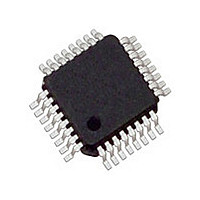
IDT5T93GL061PFI IDT, Integrated Device Technology Inc, IDT5T93GL061PFI Datasheet - Page 7

IDT5T93GL061PFI
Manufacturer Part Number
IDT5T93GL061PFI
Description
Manufacturer
IDT, Integrated Device Technology Inc
Type
Clock Driverr
Datasheet
1.IDT5T93GL061PFI.pdf
(14 pages)
Specifications of IDT5T93GL061PFI
Number Of Clock Inputs
2
Mode Of Operation
Differential
Output Frequency
450MHz
Output Logic Level
LVDS
Operating Supply Voltage (min)
2.3V
Operating Supply Voltage (typ)
2.5V
Operating Supply Voltage (max)
2.7V
Package Type
TQFP
Operating Temp Range
-40C to 85C
Operating Temperature Classification
Industrial
Mounting
Surface Mount
Pin Count
32
Quiescent Current
240mA
Lead Free Status / RoHS Status
Not Compliant
NOTES:
1. AC propagation measurements should not be taken within the first 100 cycles of startup.
2. Skew measured between crosspoints of all differential output pairs under identical input and output interfaces, transitions and load conditions on any one device.
3. Skew measured is the difference between propagation delay times t
4. Skew measured is the magnitude of the difference in propagation times between any single differential output pair of two devices, given identical transitions and load conditions
5. All parameters are tested with a 50% input duty cycle.
6. Guaranteed by design but not production tested.
AC ELECTRICAL CHARACTERISTICS OVER OPERATING RANGE
Skew Parameters
Propagation Delay
Output Gate Enable/Disable Delay
Power Down Timing
IDT5T93GL061
2.5V LVDS 1:6 GLITCHLESS CLOCK BUFFER TERABUFFER II
conditions on any one device.
at identical V
Symbol
t
t
t
PWRDN
t
t
PWRUP
SK
SK
SK
t
t
t
t
PLH
PHL
PGE
PGD
f
(
O
(
(
PP
O
P
)
)
)
DD
levels and temperature.
Parameter
Same Device Output Pin-to-Pin Skew
Pulse Skew
Part-to-Part Skew
Propagation Delay A, A Crosspoint to Qn, Qn Crosspoint
Frequency Range
Output Gate Enable Crossing V
Output Gate Disable Crossing V
PD Crossing V
Output Gate Disable Crossing V
(3)
THI
(4)
(6)
to Qn = V
DD
, Qn = V
THI
THI
THI
to Qn/Qn Crosspoint
to Qn/Qn Driven to GL Designated Level
to Qn/Qn Crosspoint Driven to GL Designated Level
PHL
(2)
DD
and t
PLH
of any single differential output pair under identical input and output interfaces, transitions and load
7
INDUSTRIAL TEMPERATURE RANGE
Min.
—
—
—
—
—
—
—
—
—
(1,5)
Typ.
1.5
—
—
—
—
—
—
—
—
Max
100
300
450
100
100
2.2
3.5
3.5
50
MHz
Unit
μS
μS
ps
ps
ps
ns
ns
ns


