ICS83948AYI IDT, Integrated Device Technology Inc, ICS83948AYI Datasheet
ICS83948AYI
Specifications of ICS83948AYI
Available stocks


Related parts for ICS83948AYI


ICS83948AYI Summary of contents
Page 1
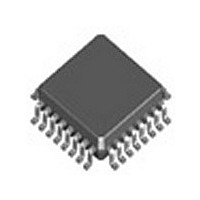
... Available in both standard (RoHS 5) and lead-free (RoHS 6) packages Q10 Q11 1 Pin Assignment CLK_SEL 1 2 LVCMOS_CLK CLK 3 4 nCLK CLK_EN GND ICS83948I 32-Lead LQFP 7mm x 7mm x 1.4mm package body Y Package Top View ICS83948AYI REV. C NOVEMBER 7, 2008 ICS83948I GND DDO Q5 21 GND DDO Q7 17 ...
Page 2
... Clock enable pin. LVCMOS/LVTTL interface levels. Input Pullup Output enable pin. LVCMOS/LVTTL interface levels. Positive supply pin. Power supply ground. Single-ended clock outputs. LVCMOS/LVTTL interface levels. Output supply pins. Test Conditions Clock LVCMOS_CLK De-selected Selected 2 Minimum Typical Maximum ICS83948AYI REV. C NOVEMBER 7, 2008 Units pF Ω k Ω Ω ...
Page 3
... Differential to Single-Ended Single-Ended to Single-Ended Single-Ended to Single-Ended Single-Ended to Single-Ended Single-Ended to Single-Ended Single-Ended to Single-Ended Single-Ended to Single-Ended + 0. 0.5V DDO = -40°C to 85°C A Minimum Typical Maximum 3.0 3.3 3.0 3.3 ICS83948AYI REV. C NOVEMBER 7, 2008 Polarity Non-Inverting Non-Inverting Non-Inverting Non-Inverting Inverting Inverting Non-Inverting Non-Inverting Units 3 ...
Page 4
... DDO /2 of the output. DDO 4 Minimum Typical 2 -0.3 0.15 GND + 0.5 2.5 Minimum Typical 2. DDO /2 DDO 0 800 Cycle /2. DDO ICS83948AYI REV. C NOVEMBER 7, 2008 Maximum Units 0 – 0. ±100 µA V 0.4 V Maximum Units 250 MHz 3. 350 ps 1.5 ...
Page 5
... IDT™ / ICS™ LVCMOS/LVTTL CLOCK GENERATOR V DD SCOPE nCLK Qx CLK GND Differential Input Level Qx Qy Output Skew 2V Q0:Q11 0. Output Pulse Width Cross Points PP V DDO 2 V DDO 2 tsk( DDO DDO PERIOD t PW odc = t PERIOD ICS83948AYI REV. C NOVEMBER 7, 2008 CMR V DDO 2 ...
Page 6
... ICS83948I LOW SKEW, 1-TO-12 DIFFERENTIAL-TO-LVCMOS/LVTTL FANOUT BUFFER Parameter Measurement Information, continued LVCMOS_CLK nCLK CLK V DDO 2 Q0:Q11 ➤ ➤ Propagation Delay IDT™ / ICS™ LVCMOS/LVTTL CLOCK GENERATOR ICS83948AYI REV. C NOVEMBER 7, 2008 6 ...
Page 7
... A 1kΩ resistor can be used. IDT™ / ICS™ LVCMOS/LVTTL CLOCK GENERATOR / Single Ended Clock Input Figure 1. Single-Ended Signal Driving Differential Input Outputs: LVCMOS Outputs All unused LVCMOS output can be left floating. There should be no trace attached CLK V_REF nCLK C1 0. ICS83948AYI REV. C NOVEMBER 7, 2008 ...
Page 8
... Zo = 50Ω R1 100 Zo = 50Ω LVDS Driven by a 3.3V LVDS Driver 2. 120 120 Zo = 60Ω 60Ω SSTL R1 R2 120 120 Driven by a 2.5V SSTL Driver ICS83948AYI REV. C NOVEMBER 7, 2008 3.3V CLK nCLK HiPerClockS Input 3.3V CLK nCLK Receiver 3.3V CLK nCLK HiPerClockS ...
Page 9
... Transistor Count The transistor count for ICS83948I is: 1040 Pin compatible with the MPC948/948L IDT™ / ICS™ LVCMOS/LVTTL CLOCK GENERATOR θ by Velocity JA 0 200 67.8°C/W 55.9°C/W 47.9°C/W 42.1°C/W 9 500 50.1°C/W 39.4°C/W ICS83948AYI REV. C NOVEMBER 7, 2008 ...
Page 10
... D & E 9.00 Basic D1 & E1 7.00 Basic D2 & E2 5.60 Ref. e 0.80 Basic L 0.45 0.60 θ 0° ccc Reference Document: JEDEC Publication 95, MS-026 IDT™ / ICS™ LVCMOS/LVTTL CLOCK GENERATOR Maximum 1.60 0.15 1.45 0.45 0.20 0.75 7° 0.10 10 ICS83948AYI REV. C NOVEMBER 7, 2008 ...
Page 11
... Shipping Packaging 32 Lead LQFP 32 Lead LQFP 1000 Tape & Reel “Lead-Free” 32 Lead LQFP “Lead-Free” 32 Lead LQFP 1000 Tape & Reel 11 Temperature Tray -40°C to 85°C -40°C to 85°C Tray -40°C to 85°C -40°C to 85°C ICS83948AYI REV. C NOVEMBER 7, 2008 ...
Page 12
... Added Differential Clock Input Interface Section. Ordering Information Table - corrected Temperature column. Updated datasheet format and PLZ PHZ ""Clock Enable Hold H Test Conditions. PW from 4pF max. to 4pF typical. IN ICS83948AYI REV. C NOVEMBER 7, 2008 Date 5/20/02 6/26/02 8/8/02 11/11/02 12/15/05 3/6/08 ...
Page 13
ICS83948I LOW SKEW, 1-TO-12 DIFFERENTIAL-TO-LVCMOS/LVTTL FANOUT BUFFER Innovate with IDT and accelerate your future networks. Contact: www.IDT.com For Sales 800-345-7015 408-284-8200 Fax: 408-284-2775 Corporate Headquarters Integrated Device Technology, Inc. 6024 Silver Creek Valley Road San Jose, CA 95138 United States ...