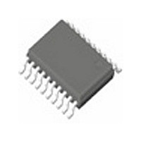
ICS853014BGT IDT, Integrated Device Technology Inc, ICS853014BGT Datasheet - Page 11

ICS853014BGT
Manufacturer Part Number
ICS853014BGT
Description
Manufacturer
IDT, Integrated Device Technology Inc
Type
Clock Driverr
Datasheet
1.ICS853014BGT.pdf
(19 pages)
Specifications of ICS853014BGT
Number Of Clock Inputs
2
Mode Of Operation
Differential
Output Frequency
>2000MHz
Output Logic Level
ECL/LVPECL
Operating Supply Voltage (min)
-2.375/2.375V
Operating Supply Voltage (typ)
-2.5/-3.3/3.3V
Operating Supply Voltage (max)
-3.8/3.8V
Package Type
TSSOP
Operating Temp Range
-40C to 85C
Operating Temperature Classification
Industrial
Signal Type
CML/LVDS/LVPECL/SSTL
Mounting
Surface Mount
Pin Count
20
Lead Free Status / RoHS Status
Not Compliant
Recommendations for Unused Output Pins
Inputs:
PCLK/nPCLK I
For applications not requiring the use of a differential input, both
the PCLK and nPCLK pins can be left floating. Though not
required, but for additional protection, a 1kW resistor can be tied
from PCLK to ground. For applications
LVCMOS Control Pins
All control pins have internal pull-ups or pull-downs; additional
resistance is not required but can be added for additional
protection. A 1k
Termination for 3.3V LVPECL Outputs
The clock layout topology shown below is a typical termination for
LVPECL outputs. The two different layouts mentioned are
recommended only as guidelines.
FOUT and nFOUT are low impedance follower outputs that
generate ECL/LVPECL compatible outputs. Therefore, terminating
resistors (DC current path to ground) or current sources must be
used for functionality. These outputs are designed to drive 50Ω
Figure 4A. 3.3V LVPECL Output Termination
IDT™ / ICS™ 2.5V, 3.3V LVPECL/ECL FANOUT BUFFER
ICS853014
LOW SKEW, 1-TO-5, DIFFERENTIAL-TO-2.5V, 3.3V LVPECL/ECL FANOUT BUFFER
RTT =
((V
FOUT
OH
Ω
+ V
NPUTS
resistor can be used.
OL
) / (V
1
CC
Z
Z
– 2)) – 2
o
o
= 50
= 50
Z
o
50
RTT
50
V
CC
FIN
- 2V
11
Outputs:
LVPECL Outputs
All unused LVPECL outputs can be left floating. We recommend
that there is no trace attached. Both sides of the differential output
pair should either be left floating or terminated.
transmission lines. Matched impedance techniques should be
used to maximize operating frequency and minimize signal
distortion. Figures 4A and 4B show two different layouts which are
recommended only as guidelines. Other suitable clock layouts may
exist and it would be recommended that the board designers
simulate to guarantee compatibility across all printed circuit and
clock component process variations.
Figure 4B. 3.3V LVPECL Output Termination
FOUT
Z
Z
ICS853014BG REV. D FEBRUARY 25, 2009
o
o
= 50
= 50
125
84
3.3V
125
84
FIN


