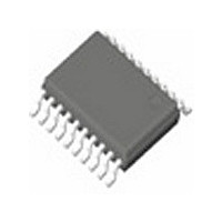
ICS853014BGT IDT, Integrated Device Technology Inc, ICS853014BGT Datasheet - Page 2

ICS853014BGT
Manufacturer Part Number
ICS853014BGT
Description
Manufacturer
IDT, Integrated Device Technology Inc
Type
Clock Driverr
Datasheet
1.ICS853014BGT.pdf
(19 pages)
Specifications of ICS853014BGT
Number Of Clock Inputs
2
Mode Of Operation
Differential
Output Frequency
>2000MHz
Output Logic Level
ECL/LVPECL
Operating Supply Voltage (min)
-2.375/2.375V
Operating Supply Voltage (typ)
-2.5/-3.3/3.3V
Operating Supply Voltage (max)
-3.8/3.8V
Package Type
TSSOP
Operating Temp Range
-40C to 85C
Operating Temperature Classification
Industrial
Signal Type
CML/LVDS/LVPECL/SSTL
Mounting
Surface Mount
Pin Count
20
Lead Free Status / RoHS Status
Not Compliant
Table 1. Pin Descriptions
NOTE: Pullup refers to internal input resistors. See Table 2, Pin Characteristics, for typical values.
Table 2. Pin Characteristics
IDT™ / ICS™ 2.5V, 3.3V LVPECL/ECL FANOUT BUFFER
Symbol
R
R
ICS853014
LOW SKEW, 1-TO-5, DIFFERENTIAL-TO-2.5V, 3.3V LVPECL/ECL FANOUT BUFFER
Number
VCC/2
PULLDOWN
18, 20
9, 10
1, 2
3, 4
5, 6
7, 8
11
12
13
14
15
16
17
19
Parameter
Input Pulldown Resistor
Pullup/Pulldown Resistors
CLK_SEL
Q0, nQ0
Q1, nQ1
Q2, nQ2
Q3, nQ3
Q4, nQ4
nPCLK0
nPCLK1
PCLK0
PCLK1
Name
nEN
V
V
V
CC
EE
BB
Output
Output
Output
Output
Output
Output
Power
Power
Input
Input
Input
Input
Input
Input
Type
Pulldown
Pulldown
Pulldown
Pulldown
Pulldown
Pulldown
Pullup/
Pullup/
Test Conditions
Description
Differential output pair. LVPECL/ECL interface levels.
Differential output pair. LVPECL/ECL interface levels.
Differential output pair. LVPECL/ECL interface levels.
Differential output pair. LVPECL/ECL interface levels.
Differential output pair. LVPECL/ECL interface levels.
Negative supply pin.
Clock select input. When HIGH, selects PCLK1/nPCLK1 inputs. When LOW,
selects PCLK0/nPCLK0 inputs. Single-ended LVPECL interface levels.
Non-inverting differential LVPECL clock input.
Inverting differential LVPECL clock input. V
Bias voltage.
Non-inverting differential LVPECL clock input.
Inverting differential LVPECL clock input. V
Positive supply pins.
Synchronizing clock enable. When LOW, clock outputs follow clock input. When
HIGH, Qx outputs are forced low, nQx outputs are forced high.
Single-ended LVPECL interface levels.
2
Minimum
ICS853014BG REV. D FEBRUARY 25, 2009
Typical
CC
CC
75
50
/2 default when left floating.
/2 default when left floating.
Maximum
Units
k
k
Ω
Ω


