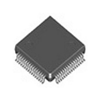
IDT77V106L25TFI IDT, Integrated Device Technology Inc, IDT77V106L25TFI Datasheet - Page 11

IDT77V106L25TFI
Manufacturer Part Number
IDT77V106L25TFI
Description
Manufacturer
IDT, Integrated Device Technology Inc
Datasheet
1.IDT77V106L25TFI.pdf
(27 pages)
Specifications of IDT77V106L25TFI
Data Rate
25.6/51.2Mbps
Number Of Channels
1
Type Of Atm Phy Interface
UTOPIA
Operating Supply Voltage (typ)
3.3V
Operating Supply Voltage (min)
3V
Operating Supply Voltage (max)
3.6V
Operating Temp Range
-40C to 85C
Operating Temperature Classification
Industrial
Pin Count
64
Mounting
Surface Mount
Lead Free Status / RoHS Status
Not Compliant
Available stocks
Company
Part Number
Manufacturer
Quantity
Price
Company:
Part Number:
IDT77V106L25TFI
Manufacturer:
NEC
Quantity:
4 102
Part Number:
IDT77V106L25TFI
Manufacturer:
IDT
Quantity:
20 000
CONTROL AND STATUS INTERFACE
Utility Bus
within the IDT77V106. These registers are used to select desired operating
characteristics and functions, and to communicate status to external systems.
(AD[7:0]) where the register address is latched via the Address Latch Enable
(ALE) signal.
Read Operation
Refer to the Utility Bus timing waveforms. A register read is performed as follows:
Write Operation
A register write is performed as described below:
IDT77V106L25
The Utility Bus is a byte-wide interface that provides access to the registers
The Utility Bus is implemented using a multiplexed address and data bus
The Utility Bus interface is comprised of the following pins:
AD[7:0], ALE, CS, RD, WR
1.
2. Set up register address:
3.
1.
2.
— RD , WR , CS not asserted (logic 1)
— ALE not asserted (logic 0)
— place desired register address on AD[7:0]
— set ALE to logic 1;
— latch this address by setting ALE to logic 0.
— Remove register address data from AD[7:0]
— assert CS by setting to logic 0;
— assert RD by setting to logic 0
— wait minimum pulse width time (see AC specifications)
— RD , WR , CS not asserted (logic 1)
— ALE not asserted (logic 0)
— place desired register address on AD[7:0]
— set ALE to logic 1;
— latch this address by setting ALE to logic 0.
Initial condition:
Read register data:
Initial condition:
Set up register address:
11
Interrupt Operations
They are useful both during ‘normal’ operation, and as diagnostic aids. Refer
to the Status and Control Register List section.
When this bit is cleared (set to 0), interrupt signalling is prevented. The Interrupt
Mask Register allows individual masking of different interrupt sources. Additional
interrupt signal control is provided by bit 5 of the Master Control Register. When
this bit is set (=1), receive cell errors will be flagged via interrupt signalling and
all other interrupt conditions are masked. These errors include:
5 in the Master Control Register. INT (pin 34) will go to a low state when an
interrupt condition is detected. The external system should then interrogate the
77V106L25 to determine which one (or more) conditions caused this flag, and
reset the interrupt for further occurrences. This is accomplished by reading the
Interrupt Status Register. Decoding the bits in this byte will tell which error
condition caused the interrupt. Reading this register also:
problems.
3.
A variety of selectable interrupt and signalling conditions are provided.
Overall interrupt control is provided via bit 0 of the Master Control Register.
Normal interrupt operations are performed by setting bit 0 and clearing bit
•
This leaves the interrupt system ready to signal an alarm for further
— place data on AD[7:0]
— assert CS by setting to logic 0;
— assert WR (logic 0) for minimum time (according to timing
specification); reset WR or CS to logic 1 to complete register write
cycle.
•
•
•
•
resets INT
clears the (sticky) interrupt status bits in the registers that are read
Write data:
Bad receive HEC
Short (fewer than 53 bytes) cells
Received cell symbol error


