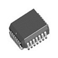
IDT82V1671J IDT, Integrated Device Technology Inc, IDT82V1671J Datasheet - Page 36

IDT82V1671J
Manufacturer Part Number
IDT82V1671J
Description
Manufacturer
IDT, Integrated Device Technology Inc
Datasheet
1.IDT82V1671J.pdf
(107 pages)
Specifications of IDT82V1671J
Number Of Channels
4
On-hook Transmission
Yes
Polarity Reversal
Yes
On-chip Ring Relay Driver
Yes
Operating Supply Voltage (typ)
3.3V
Operating Temp Range
-40C to 85C
Package Type
PLCC
Operating Temperature Classification
Industrial
Pin Count
28
Mounting
Surface Mount
Operating Current
95mA
Operating Supply Voltage (max)
3.465V
Operating Supply Voltage (min)
3.135V
Lead Free Status / RoHS Status
Not Compliant
Available stocks
Company
Part Number
Manufacturer
Quantity
Price
Company:
Part Number:
IDT82V1671J
Manufacturer:
BROADCOM
Quantity:
457
Part Number:
IDT82V1671J
Manufacturer:
IDT
Quantity:
20 000
3.7.3.3
UTD unit.
channel by the UTD_EN in register LREG8. The UTD_SRC bit in
LREG8 determines whether the signal from transmit or receive path is
detected. The RTime, RBRKTime, ETime and EBRKTime of the UTD
are programmed by LREG14, LREG15, LREG16 and LREG17,
respectively.
and the bandstop filters and the thresholds of the signal are
programmable via the Coe-RAM. The center frequencies of the two
filters should be the same. The center frequency can be programmed
Table - 10 Registers and Coe-RAM Locations Used for UTD
UTD Unit Enable
UTD Source Selection
UTD Result Indication
UTD RTime
UTD RBRKTime
UTD ETime
UTD EBRKTime
UTD Filter Coefficients and Signal
Thresholds Selection
UTD Bandpass Filter Coefficient
UTD Bandstop Filter Coefficient
UTD Signal Ceiling Threshold
UTD Signal Floor Threshold
RSLIC & CODEC CHIPSET
Table - 10
The UTD unit can be enabled or disabled individually for each
If the UTD bit in LREG5 is set to 0, the coefficients of the bandpass
Parameter
UTD Programming
shows the registers and Coe-RAM locations used for the
Bit UTD_EN in LREG8
Bit UTD_SRC in LREG8
Bit UTD_OK in LREG21
Bits UTD_RT[7:0] (LREG14)
Bits UTD_RBK[7:0] (LREG15)
Bits UTD_ET[7:0] (LREG16)
Bits UTD_EBRK[7:0] (LREG17)
Bit UTD in LREG5
UTD Bandpass Filter Coefficient in the Coe-RAM
UTD Bandstop Filter Coefficient in the Coe-RAM
UTDthld_Ceiling in the Coe-RAM
UTDthld_Floor in the Coe-RAM
Register Bits/Coe-RAM Words
36
from 1500 Hz to 2600 Hz. The bandwidths of the two filters are also
programmable. The ceiling and floor thresholds of the signal can be
programmed from
coefficients. When users input the desired center frequency, bandwidth
for the two filters and ceiling threshold, floor threshold for the signal, the
software will automatically calculate all the coefficients for the UTD unit.
After loading these coefficients to the Coe-RAM, the performance of the
UTD unit will meet the users’ requirements. Refer to
62
the ROM are used. These values are used by default. See
details.
for the Coe-RAM mapping.
IDT provides a software (Cal74) to calculate the filter and threshold
If the UTD bit is set to 1, the filter coefficients and the thresholds in
UTD_EN = 0: the UTD unit is disabled;
UTD_EN = 1: the UTD unit is enabled.
UTD_SRC = 0: signal from receive path is detected;
UTD_SRC = 1: signal from transmit path is detected.
UTD_OK = 0: no fax/modem tone has been detected;
UTD_OK = 1: fax/modem tone has been detected.
Recognition time, programmable from 0 to 4000 ms. The default value is
304 ms.
Recognition break time, programmable from 0 to 1000 ms. The default
value is 100 ms.
End detection time, programmable from 0 to 1000 ms. The default value is
256 ms.
End detection break time, programmable from 0 to 255 ms. The default
value is 100 ms.
UTD = 0: The signal thresholds and filter coefficients written in the Coe-
RAM are selected.
UTD = 1: The signal thresholds and filter coefficients in the ROM are
selected (default);
The center frequency is programmable from 1500 Hz to 2600 Hz. The
default center frequency and bandwidth (in the ROM) are 2100 Hz and 60
Hz respectively.
The center frequency is programmable from 1500 Hz to 2600 Hz. The
default center frequency and bandwidth (in the ROM) are 2100 Hz and
230 Hz respectively.
Programmable from −30 dBm to 0 dBm in minimum steps of 0.2 dBm. The
default value (in the ROM) is −6 dBm.
Programmable from −30 dBm to 0 dBm in minimum steps of 0.2 dBm. The
default value (in the ROM) is −18 dBm.
−30 dBm to 0 dBm in minimum steps of 0.2 dBm.
IDT82V1671/IDT82V1671A, IDT82V1074
Notes
Table - 23 on page
Table - 10 for


