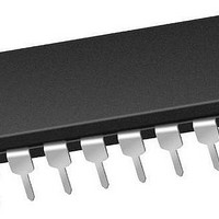
PIC16F1829-E/P Microchip Technology, PIC16F1829-E/P Datasheet - Page 167

PIC16F1829-E/P
Manufacturer Part Number
PIC16F1829-E/P
Description
14 KB Flash, 1K Bytes RAM, 32 MHz Int. Osc, 18 I/0, Enhanced Mid Range Core 20 P
Manufacturer
Microchip Technology
Series
PIC® XLP™ mTouch™ 16Fr
Datasheet
1.PIC16LF1829-ISO.pdf
(420 pages)
Specifications of PIC16F1829-E/P
Core Processor
PIC
Core Size
8-Bit
Speed
32MHz
Connectivity
I²C, LIN, SPI, UART/USART
Peripherals
Brown-out Detect/Reset, POR, PWM, WDT
Number Of I /o
17
Program Memory Size
14KB (8K x 14)
Program Memory Type
FLASH
Eeprom Size
256 x 8
Ram Size
1K x 8
Voltage - Supply (vcc/vdd)
1.8 V ~ 5.5 V
Data Converters
A/D 12x10b
Oscillator Type
Internal
Operating Temperature
-40°C ~ 125°C
Package / Case
*
Processor Series
PIC16F182x
Core
PIC
Data Bus Width
8 bit
Data Ram Size
1 KB
Interface Type
I2C, SPI, USART
Maximum Clock Frequency
32 MHz
Number Of Programmable I/os
18
Number Of Timers
5
Operating Supply Voltage
1.8 V to 5.5 V
Maximum Operating Temperature
+ 125 C
Mounting Style
Through Hole
Lead Free Status / RoHS Status
Lead free / RoHS Compliant
Lead Free Status / RoHS Status
Lead free / RoHS Compliant
- Current page: 167 of 420
- Download datasheet (5Mb)
17.4
In order for the DAC module to consume the least
amount of power, one of the two voltage reference input
sources to the resistor ladder must be disconnected.
Either the positive voltage source, (V
negative voltage source, (V
The negative voltage source is disabled by setting the
DACLPS bit in the DACCON0 register. Clearing the
DACLPS bit in the DACCON0 register disables the
positive voltage source.
17.4.1
The DAC output voltage can be set to V
least amount of power consumption by performing the
following:
• Clearing the DACEN bit in the DACCON0 register.
• Setting the DACLPS bit in the DACCON0 register.
• Configuring the DACPSS bits to the proper
• Configuring the DACR<4:0> bits to ‘11111’ in the
FIGURE 17-3:
17.5
When the device wakes up from Sleep through an
interrupt or a Watchdog Timer time-out, the contents of
the DACCON0 register are not affected. To minimize
current consumption in Sleep mode, the voltage
reference should be disabled.
17.6
A device Reset affects the following:
• DAC is disabled.
• DAC output voltage is removed from the
• The DACR<4:0> range select bits are cleared.
2010 Microchip Technology Inc.
positive source.
DACCON1 register.
DACOUT pin.
Output Clamped to Positive Voltage Source
DACEN = 0
DACLPS = 1
V
V
SRC
SRC
Low-Power Voltage State
Operation During Sleep
Effects of a Reset
OUTPUT CLAMPED TO POSITIVE
VOLTAGE SOURCE
+
-
OUTPUT VOLTAGE CLAMPING EXAMPLES
SRC
R
R
R
-) can be disabled.
DACR<4:0> = 11111
DAC Voltage Ladder
(see
Figure
SRC
SRC
+), or the
+ with the
17-1)
Preliminary
This is also the method used to output the voltage level
from the FVR to an output pin. See
“Operation During Sleep”
Reference
17.4.2
The DAC output voltage can be set to V
least amount of power consumption by performing the
following:
• Clearing the DACEN bit in the DACCON0 register.
• Clearing the DACLPS bit in the DACCON0 register.
• Configuring the DACNSS bits to the proper
• Configuring the DACR<4:0> bits to ‘00000’ in the
This allows the comparator to detect a zero-crossing
while not consuming additional current through the DAC
module.
Reference
Output Clamped to Negative Voltage Source
PIC16F/LF1825/1829
negative source.
DACCON1 register.
DACEN = 0
DACLPS = 0
V
V
SRC
SRC
+
-
Figure 17-3
Figure 17-3
OUTPUT CLAMPED TO NEGATIVE
VOLTAGE SOURCE
for output clamping examples.
for output clamping examples.
R
R
R
for more information.
DACR<4:0> = 00000
DAC Voltage Ladder
(see
Figure
DS41440A-page 167
SRC
Section 17.5
17-1)
- with the
Related parts for PIC16F1829-E/P
Image
Part Number
Description
Manufacturer
Datasheet
Request
R

Part Number:
Description:
IC, 8BIT MCU, PIC16F, 32MHZ, SOIC-18
Manufacturer:
Microchip Technology
Datasheet:

Part Number:
Description:
IC, 8BIT MCU, PIC16F, 32MHZ, SSOP-20
Manufacturer:
Microchip Technology
Datasheet:

Part Number:
Description:
IC, 8BIT MCU, PIC16F, 32MHZ, DIP-18
Manufacturer:
Microchip Technology
Datasheet:

Part Number:
Description:
IC, 8BIT MCU, PIC16F, 32MHZ, QFN-28
Manufacturer:
Microchip Technology
Datasheet:

Part Number:
Description:
IC, 8BIT MCU, PIC16F, 32MHZ, QFN-28
Manufacturer:
Microchip Technology
Datasheet:

Part Number:
Description:
IC, 8BIT MCU, PIC16F, 32MHZ, QFN-28
Manufacturer:
Microchip Technology
Datasheet:

Part Number:
Description:
IC, 8BIT MCU, PIC16F, 32MHZ, SSOP-20
Manufacturer:
Microchip Technology
Datasheet:

Part Number:
Description:
IC, 8BIT MCU, PIC16F, 20MHZ, DIP-40
Manufacturer:
Microchip Technology
Datasheet:

Part Number:
Description:
IC, 8BIT MCU, PIC16F, 32MHZ, QFN-28
Manufacturer:
Microchip Technology
Datasheet:

Part Number:
Description:
IC, 8BIT MCU, PIC16F, 20MHZ, MQFP-44
Manufacturer:
Microchip Technology
Datasheet:

Part Number:
Description:
IC, 8BIT MCU, PIC16F, 20MHZ, QFN-20
Manufacturer:
Microchip Technology
Datasheet:

Part Number:
Description:
IC, 8BIT MCU, PIC16F, 32MHZ, QFN-28
Manufacturer:
Microchip Technology
Datasheet:

Part Number:
Description:
MCU 14KB FLASH 768B RAM 64-TQFP
Manufacturer:
Microchip Technology
Datasheet:

Part Number:
Description:
7 KB Flash, 384 Bytes RAM, 32 MHz Int. Osc, 16 I/0, Enhanced Mid Range Core, Low
Manufacturer:
Microchip Technology

Part Number:
Description:
14KB Flash, 512B RAM, 256B EEPROM, LCD, 1.8-5.5V 40 UQFN 5x5x0.5mm TUBE
Manufacturer:
Microchip Technology
Datasheet:


