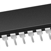
PIC16F1829-E/P Microchip Technology, PIC16F1829-E/P Datasheet - Page 183

PIC16F1829-E/P
Manufacturer Part Number
PIC16F1829-E/P
Description
14 KB Flash, 1K Bytes RAM, 32 MHz Int. Osc, 18 I/0, Enhanced Mid Range Core 20 P
Manufacturer
Microchip Technology
Series
PIC® XLP™ mTouch™ 16Fr
Datasheet
1.PIC16LF1829-ISO.pdf
(420 pages)
Specifications of PIC16F1829-E/P
Core Processor
PIC
Core Size
8-Bit
Speed
32MHz
Connectivity
I²C, LIN, SPI, UART/USART
Peripherals
Brown-out Detect/Reset, POR, PWM, WDT
Number Of I /o
17
Program Memory Size
14KB (8K x 14)
Program Memory Type
FLASH
Eeprom Size
256 x 8
Ram Size
1K x 8
Voltage - Supply (vcc/vdd)
1.8 V ~ 5.5 V
Data Converters
A/D 12x10b
Oscillator Type
Internal
Operating Temperature
-40°C ~ 125°C
Package / Case
*
Processor Series
PIC16F182x
Core
PIC
Data Bus Width
8 bit
Data Ram Size
1 KB
Interface Type
I2C, SPI, USART
Maximum Clock Frequency
32 MHz
Number Of Programmable I/os
18
Number Of Timers
5
Operating Supply Voltage
1.8 V to 5.5 V
Maximum Operating Temperature
+ 125 C
Mounting Style
Through Hole
Lead Free Status / RoHS Status
Lead free / RoHS Compliant
Lead Free Status / RoHS Status
Lead free / RoHS Compliant
- Current page: 183 of 420
- Download datasheet (5Mb)
REGISTER 19-2:
REGISTER 19-3:
2010 Microchip Technology Inc.
bit 7
Legend:
R = Readable bit
u = Bit is unchanged
‘1’ = Bit is set
bit 7
bit 6
bit 5-4
bit 3-2
bit 1-0
bit 7
Legend:
R = Readable bit
u = Bit is unchanged
‘1’ = Bit is set
bit 7-2
bit 1
bit 0
R/W-0/0
CxINTP
U-0
—
CxINTP: Comparator Interrupt on Positive Going Edge Enable bits
1 = The CxIF interrupt flag will be set upon a positive going edge of the CxOUT bit
0 = No interrupt flag will be set on a positive going edge of the CxOUT bit
CxINTN: Comparator Interrupt on Negative Going Edge Enable bits
1 = The CxIF interrupt flag will be set upon a negative going edge of the CxOUT bit
0 = No interrupt flag will be set on a negative going edge of the CxOUT bit
CxPCH<1:0>: Comparator Positive Input Channel Select bits
00 = CxVP connects to CxIN+ pin
01 = CxVP connects to DAC Voltage Reference
10 = CxVP connects to FVR Voltage Reference
For C1:
11 = CxVP connects to C12IN+ pin
For C2:
11 = CxVP connects to V
Unimplemented: Read as ‘0’
CxNCH<1:0>: Comparator Negative Input Channel Select bits
00 = CxVN connects to C12IN0- pin
01 = CxVN connects to C12IN1- pin
10 = CxVN connects to C12IN2- pin
11 = CxVN connects to C12IN3- pin
Unimplemented: Read as ‘0’
MC2OUT: Mirror Copy of C2OUT bit
MC1OUT: Mirror Copy of C1OUT bit
R/W-0/0
CxINTN
U-0
—
CMxCON1: COMPARATOR Cx CONTROL REGISTER 1
CMOUT: COMPARATOR OUTPUT REGISTER
W = Writable bit
x = Bit is unknown
‘0’ = Bit is cleared
W = Writable bit
x = Bit is unknown
‘0’ = Bit is cleared
R/W-0/0
U-0
—
CxPCH<1:0>
SS
R/W-0/0
U-0
Preliminary
—
U = Unimplemented bit, read as ‘0’
-n/n = Value at POR and BOR/Value at all other Resets
U = Unimplemented bit, read as ‘0’
-n/n = Value at POR and BOR/Value at all other Resets
PIC16F/LF1825/1829
U-0
U-0
—
—
U-0
U-0
—
—
MC2OUT
R/W-0/0
R-0/0
CxNCH<1:0>
DS41440A-page 183
MC1OUT
R/W-0/0
R-0/0
bit 0
bit 0
Related parts for PIC16F1829-E/P
Image
Part Number
Description
Manufacturer
Datasheet
Request
R

Part Number:
Description:
IC, 8BIT MCU, PIC16F, 32MHZ, SOIC-18
Manufacturer:
Microchip Technology
Datasheet:

Part Number:
Description:
IC, 8BIT MCU, PIC16F, 32MHZ, SSOP-20
Manufacturer:
Microchip Technology
Datasheet:

Part Number:
Description:
IC, 8BIT MCU, PIC16F, 32MHZ, DIP-18
Manufacturer:
Microchip Technology
Datasheet:

Part Number:
Description:
IC, 8BIT MCU, PIC16F, 32MHZ, QFN-28
Manufacturer:
Microchip Technology
Datasheet:

Part Number:
Description:
IC, 8BIT MCU, PIC16F, 32MHZ, QFN-28
Manufacturer:
Microchip Technology
Datasheet:

Part Number:
Description:
IC, 8BIT MCU, PIC16F, 32MHZ, QFN-28
Manufacturer:
Microchip Technology
Datasheet:

Part Number:
Description:
IC, 8BIT MCU, PIC16F, 32MHZ, SSOP-20
Manufacturer:
Microchip Technology
Datasheet:

Part Number:
Description:
IC, 8BIT MCU, PIC16F, 20MHZ, DIP-40
Manufacturer:
Microchip Technology
Datasheet:

Part Number:
Description:
IC, 8BIT MCU, PIC16F, 32MHZ, QFN-28
Manufacturer:
Microchip Technology
Datasheet:

Part Number:
Description:
IC, 8BIT MCU, PIC16F, 20MHZ, MQFP-44
Manufacturer:
Microchip Technology
Datasheet:

Part Number:
Description:
IC, 8BIT MCU, PIC16F, 20MHZ, QFN-20
Manufacturer:
Microchip Technology
Datasheet:

Part Number:
Description:
IC, 8BIT MCU, PIC16F, 32MHZ, QFN-28
Manufacturer:
Microchip Technology
Datasheet:

Part Number:
Description:
MCU 14KB FLASH 768B RAM 64-TQFP
Manufacturer:
Microchip Technology
Datasheet:

Part Number:
Description:
7 KB Flash, 384 Bytes RAM, 32 MHz Int. Osc, 16 I/0, Enhanced Mid Range Core, Low
Manufacturer:
Microchip Technology

Part Number:
Description:
14KB Flash, 512B RAM, 256B EEPROM, LCD, 1.8-5.5V 40 UQFN 5x5x0.5mm TUBE
Manufacturer:
Microchip Technology
Datasheet:


