PIC16LF1903T-I/SO Microchip Technology, PIC16LF1903T-I/SO Datasheet - Page 83
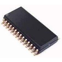
PIC16LF1903T-I/SO
Manufacturer Part Number
PIC16LF1903T-I/SO
Description
7KB Flash, 256B RAM, LCD, 11x10b ADC, NanoWatt XLP 28 SOIC .300in T/R
Manufacturer
Microchip Technology
Series
PIC® XLP™ 16Fr
Datasheet
1.PIC16LF1902-EMV.pdf
(240 pages)
Specifications of PIC16LF1903T-I/SO
Processor Series
PIC16LF190x
Core
PIC
Data Bus Width
8 bit
Program Memory Type
Flash
Program Memory Size
4 KB
Data Ram Size
256 B
Maximum Clock Frequency
20 MHz
Number Of Programmable I/os
25
Number Of Timers
2
Operating Supply Voltage
1.8 V to 3.6 V
Maximum Operating Temperature
+ 85 C
Mounting Style
SMD/SMT
Package / Case
SOIC-28
Core Processor
PIC
Core Size
8-Bit
Speed
20MHz
Connectivity
-
Peripherals
Brown-out Detect/Reset, LCD, POR, PWM, WDT
Number Of I /o
25
Eeprom Size
-
Ram Size
256 x 8
Voltage - Supply (vcc/vdd)
1.8 V ~ 3.6 V
Data Converters
A/D 11x10b
Oscillator Type
Internal
Operating Temperature
-40°C ~ 85°C
Lead Free Status / Rohs Status
Details


10.2.3
While executing code, program memory can only be
erased by rows. To erase a row:
1.
2.
3.
4.
5.
See
After the “BSF PMCON1,WR” instruction, the processor
requires two cycles to set up the erase operation. The
user must place two NOP instructions after the WR bit is
set. The processor will halt internal operations for the
typical 2 ms erase time. This is not Sleep mode as the
clocks and peripherals will continue to run. After the
erase cycle, the processor will resume operation with
the third instruction after the PMCON1 WRITE instruc-
tion.
2011 Microchip Technology Inc.
Load the PMADRH:PMADRL register pair with
any address within the row to be erased.
Clear the CFGS bit of the PMCON1 register.
Set the FREE and WREN bits of the PMCON1
register.
Write 55h, then AAh, to PMCON2 (Flash
programming unlock sequence).
Set control bit WR of the PMCON1 register to
begin the erase operation.
Example
ERASING FLASH PROGRAM
MEMORY
10-2.
Preliminary
FIGURE 10-4:
Program or Configuration Memory
Disable Write/Erase Operation
Enable Write/Erase Operation
PIC16LF1902/3
Erase operation completes
Select Erase Operation
(PMADRH:PMADRL)
Re-enable Interrupts
Select Row Address
Disable Interrupts
Unlock Sequence
Erase Operation
CPU stalls while
Erase Operation
(FIGURE x-x)
(2ms typical)
(WREN = 1)
(WREN = 0)
FLASH PROGRAM
MEMORY ERASE
FLOWCHART
(FREE = 1)
Figure 10-3
(GIE = 0)
(GIE = 1)
(CFGS)
Select
Start
End
DS41455B-page 83
Related parts for PIC16LF1903T-I/SO
Image
Part Number
Description
Manufacturer
Datasheet
Request
R

Part Number:
Description:
IC, 8BIT MCU, PIC16LF, 32MHZ, QFN-28
Manufacturer:
Microchip Technology
Datasheet:

Part Number:
Description:
IC, 8BIT MCU, PIC16LF, 32MHZ, QFN-28
Manufacturer:
Microchip Technology
Datasheet:

Part Number:
Description:
IC, 8BIT MCU, PIC16LF, 32MHZ, DIP-18
Manufacturer:
Microchip Technology
Datasheet:

Part Number:
Description:
IC, 8BIT MCU, PIC16LF, 20MHZ, TQFP-44
Manufacturer:
Microchip Technology
Datasheet:
Part Number:
Description:
7 KB Flash, 384 Bytes RAM, 32 MHz Int. Osc, 16 I/0, Enhanced Mid Range Core, Nan
Manufacturer:
Microchip Technology

Part Number:
Description:
14KB Flash, 512B RAM, LCD, 11x10b ADC, EUSART, NanoWatt XLP 28 SOIC .300in T/R
Manufacturer:
Microchip Technology
Datasheet:
Part Number:
Description:
14KB Flash, 512B RAM, LCD, 11x10b ADC, EUSART, NanoWatt XLP 28 SSOP .209in T/R
Manufacturer:
Microchip Technology
Datasheet:
Part Number:
Description:
MCU PIC 14KB FLASH XLP 28-SSOP
Manufacturer:
Microchip Technology
Part Number:
Description:
MCU PIC 14KB FLASH XLP 28-SOIC
Manufacturer:
Microchip Technology
Part Number:
Description:
MCU PIC 512B FLASH XLP 28-UQFN
Manufacturer:
Microchip Technology
Part Number:
Description:
MCU PIC 14KB FLASH XLP 28-SPDIP
Manufacturer:
Microchip Technology

Part Number:
Description:
MCU 7KB FLASH 256B RAM 40-UQFN
Manufacturer:
Microchip Technology
Part Number:
Description:
MCU 7KB FLASH 256B RAM 44-TQFP
Manufacturer:
Microchip Technology

Part Number:
Description:
MCU 14KB FLASH 1KB RAM 28-UQFN
Manufacturer:
Microchip Technology
Part Number:
Description:
MCU PIC 14KB FLASH XLP 40-UQFN
Manufacturer:
Microchip Technology