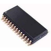
PIC18F25K80T-I/SO Microchip Technology, PIC18F25K80T-I/SO Datasheet - Page 486

PIC18F25K80T-I/SO
Manufacturer Part Number
PIC18F25K80T-I/SO
Description
ECAN, 32KB Flash, 4KB RAM, 16 MIPS, 12-bit ADC, CTMU 28 SOIC .300in T/R
Manufacturer
Microchip Technology
Series
PIC® XLP™ 18Fr
Datasheet
1.PIC18F25K80-ISO.pdf
(628 pages)
Specifications of PIC18F25K80T-I/SO
Core Processor
PIC
Core Size
8-Bit
Speed
64MHz
Connectivity
ECAN, I²C, LIN, SPI, UART/USART
Peripherals
Brown-out Detect/Reset, LVD, POR, PWM, WDT
Number Of I /o
24
Program Memory Size
32KB (16K x 16)
Program Memory Type
FLASH
Eeprom Size
1K x 8
Ram Size
3.6K x 8
Voltage - Supply (vcc/vdd)
1.8 V ~ 5.5 V
Data Converters
A/D 8x12b
Oscillator Type
Internal
Operating Temperature
-40°C ~ 85°C
Package / Case
*
Processor Series
PIC18F25K80
Core
PIC
Data Bus Width
8 bit
Data Ram Size
1 KB
Interface Type
I2C, SPI, USART
Maximum Clock Frequency
64 MHz
Number Of Programmable I/os
24
Number Of Timers
5
Operating Supply Voltage
1.8 V to 5.5 V
Maximum Operating Temperature
+ 85 C
Mounting Style
SMD/SMT
Lead Free Status / RoHS Status
Lead free / RoHS Compliant
Lead Free Status / RoHS Status
Lead free / RoHS Compliant
- Current page: 486 of 628
- Download datasheet (6Mb)
PIC18F66K80 FAMILY
28.6.2
The entire data EEPROM is protected from external
reads and writes by two bits: CPD and WRTD. CPD
inhibits external reads and writes of data EEPROM.
WRTD inhibits internal and external writes to data
EEPROM. The CPU can always read data EEPROM
under normal operation, regardless of the protection bit
settings.
28.6.3
The Configuration registers can be write-protected.
The WRTC bit controls protection of the Configuration
registers. In normal execution mode, the WRTC bit is
readable only. WRTC can only be written via ICSP or
an external programmer.
28.7
Eight memory locations (200000h-200007h) are
designated as ID locations, where the user can store
checksum or other code identification numbers. These
locations are both readable and writable during normal
execution through the TBLRD and TBLWT instructions
or during program/verify. The ID locations can be read
when the device is code-protected.
DS39977C-page 486
ID Locations
DATA EEPROM
CODE PROTECTION
CONFIGURATION REGISTER
PROTECTION
Preliminary
28.8
The PIC18F66K80 family of devices can be serially
programmed while in the end application circuit. This is
simply done with two lines for clock and data and three
other lines for power, ground and the programming
voltage. This allows customers to manufacture boards
with unprogrammed devices and then program the
microcontroller just before shipping the product. This
also allows the most recent firmware or a custom
firmware to be programmed.
For the various programming modes, see the
programming specification
28.9
When the DEBUG Configuration bit is programmed to
a ‘ 0 ’, the In-Circuit Debugger functionality is enabled.
This function allows simple debugging functions when
used with MPLAB
this feature enabled, some resources are not available
for general use.
required by the background debugger.
TABLE 28-5:
To use the In-Circuit Debugger function of the micro-
controller, the design must implement In-Circuit Serial
Programming connections to MCLR/RE3, V
RB7 and RB6. This will interface to the In-Circuit
Debugger module available from Microchip or one of
the third-party development tool companies.
I/O Pins:
Stack:
Program Memory:
Data Memory:
In-Circuit Debugger
In-Circuit Serial Programming
Table 28-5
®
DEBUGGER RESOURCES
IDE. When the microcontroller has
2011 Microchip Technology Inc.
shows which resources are
RB6, RB7
Two levels
512 bytes
10 bytes
DD
, V
SS
,
Related parts for PIC18F25K80T-I/SO
Image
Part Number
Description
Manufacturer
Datasheet
Request
R

Part Number:
Description:
Manufacturer:
Microchip Technology Inc.
Datasheet:

Part Number:
Description:
Manufacturer:
Microchip Technology Inc.
Datasheet:

Part Number:
Description:
Manufacturer:
Microchip Technology Inc.
Datasheet:

Part Number:
Description:
Manufacturer:
Microchip Technology Inc.
Datasheet:

Part Number:
Description:
Manufacturer:
Microchip Technology Inc.
Datasheet:

Part Number:
Description:
Manufacturer:
Microchip Technology Inc.
Datasheet:

Part Number:
Description:
Manufacturer:
Microchip Technology Inc.
Datasheet:

Part Number:
Description:
Manufacturer:
Microchip Technology Inc.
Datasheet:


