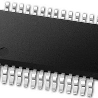
PIC24FJ32GA102-E/SS Microchip Technology, PIC24FJ32GA102-E/SS Datasheet - Page 259

PIC24FJ32GA102-E/SS
Manufacturer Part Number
PIC24FJ32GA102-E/SS
Description
16-bit, 16 MIPS, 32KB Flash, 8KB RAM, Nanowatt XLP 28 SSOP .209in TUBE
Manufacturer
Microchip Technology
Series
PIC® XLP™ 24Fr
Datasheet
1.PIC24FJ32GA102-ISP.pdf
(308 pages)
Specifications of PIC24FJ32GA102-E/SS
Processor Series
PIC24
Core
PIC24F
Data Bus Width
16 bit
Program Memory Type
Flash
Program Memory Size
32 KB
Data Ram Size
8192 B
Interface Type
I2C, SPI, UART
Maximum Clock Frequency
32 MHz
Number Of Programmable I/os
21
Number Of Timers
5
Operating Supply Voltage
2 V to 3.6 V
Maximum Operating Temperature
+ 125 C
Mounting Style
SMD/SMT
Package / Case
SSOP-28
Development Tools By Supplier
MPLAB Integrated Development Environment
Minimum Operating Temperature
- 40 C
Operating Temperature Range
- 40 C to + 125 C
Supply Current (max)
300 mA
Core Processor
PIC
Core Size
16-Bit
Speed
32MHz
Connectivity
I²C, IrDA, SPI, UART/USART
Peripherals
Brown-out Detect/Reset, LVD, POR, PWM, WDT
Number Of I /o
21
Eeprom Size
-
Ram Size
8K x 8
Voltage - Supply (vcc/vdd)
2 V ~ 3.6 V
Data Converters
A/D 10x10b
Oscillator Type
Internal
Operating Temperature
-40°C ~ 125°C
Lead Free Status / Rohs Status
Details
- Current page: 259 of 308
- Download datasheet (3Mb)
TABLE 27-2:
2010 Microchip Technology Inc.
GOTO
INC
INC2
IOR
LNK
LSR
MOV
MUL
NEG
NOP
POP
PUSH
Mnemonic
Assembly
GOTO
GOTO
INC
INC
INC
INC2
INC2
INC2
IOR
IOR
IOR
IOR
IOR
LNK
LSR
LSR
LSR
LSR
LSR
MOV
MOV
MOV
MOV
MOV
MOV.b
MOV
MOV
MOV
MOV
MOV.D
MOV.D
MUL.SS
MUL.SU
MUL.US
MUL.UU
MUL.SU
MUL.UU
MUL
NEG
NEG
NEG
NOP
NOPR
POP
POP
POP.D
POP.S
PUSH
PUSH
PUSH.D
PUSH.S
INSTRUCTION SET OVERVIEW (CONTINUED)
Expr
Wn
f
f,WREG
Ws,Wd
f
f,WREG
Ws,Wd
f
f,WREG
#lit10,Wn
Wb,Ws,Wd
Wb,#lit5,Wd
#lit14
f
f,WREG
Ws,Wd
Wb,Wns,Wnd
Wb,#lit5,Wnd
f,Wn
[Wns+Slit10],Wnd
f
f,WREG
#lit16,Wn
#lit8,Wn
Wn,f
Wns,[Wns+Slit10]
Wso,Wdo
WREG,f
Wns,Wd
Ws,Wnd
Wb,Ws,Wnd
Wb,Ws,Wnd
Wb,Ws,Wnd
Wb,Ws,Wnd
Wb,#lit5,Wnd
Wb,#lit5,Wnd
f
f
f,WREG
Ws,Wd
f
Wdo
Wnd
f
Wso
Wns
Assembly Syntax
PIC24FJ64GA104 FAMILY
Go to Address
Go to Indirect
f = f + 1
WREG = f + 1
Wd = Ws + 1
f = f + 2
WREG = f + 2
Wd = Ws + 2
f = f .IOR. WREG
WREG = f .IOR. WREG
Wd = lit10 .IOR. Wd
Wd = Wb .IOR. Ws
Wd = Wb .IOR. lit5
Link Frame Pointer
f = Logical Right Shift f
WREG = Logical Right Shift f
Wd = Logical Right Shift Ws
Wnd = Logical Right Shift Wb by Wns
Wnd = Logical Right Shift Wb by lit5
Move f to Wn
Move [Wns + Slit10] to Wnd
Move f to f
Move f to WREG
Move 16-bit Literal to Wn
Move 8-bit Literal to Wn
Move Wn to f
Move Wns to [Wns + Slit10]
Move Ws to Wd
Move WREG to f
Move Double from W(ns):W(ns + 1) to Wd
Move Double from Ws to W(nd + 1):W(nd)
{Wnd + 1, Wnd} = Signed(Wb) * Signed(Ws)
{Wnd + 1, Wnd} = Signed(Wb) * Unsigned(Ws)
{Wnd + 1, Wnd} = Unsigned(Wb) * Signed(Ws)
{Wnd + 1, Wnd} = Unsigned(Wb) * Unsigned(Ws)
{Wnd + 1, Wnd} = Signed(Wb) * Unsigned(lit5)
{Wnd + 1, Wnd} = Unsigned(Wb) * Unsigned(lit5)
W3:W2 = f * WREG
f = f + 1
WREG = f + 1
Wd = Ws + 1
No Operation
No Operation
Pop f from Top-of-Stack (TOS)
Pop from Top-of-Stack (TOS) to Wdo
Pop from Top-of-Stack (TOS) to W(nd):W(nd + 1)
Pop Shadow Registers
Push f to Top-of-Stack (TOS)
Push Wso to Top-of-Stack (TOS)
Push W(ns):W(ns + 1) to Top-of-Stack (TOS)
Push Shadow Registers
Description
Words
# of
1
1
1
1
1
1
1
1
1
1
1
1
1
1
1
1
1
1
1
1
1
1
1
1
1
1
1
2
1
1
1
1
1
1
1
1
1
1
1
1
1
1
1
1
1
1
1
1
1
1
1
Cycles
# of
DS39951C-page 259
2
2
1
1
1
1
1
1
1
1
1
1
1
1
1
1
1
1
1
1
1
1
1
1
1
1
1
1
1
2
2
1
1
1
1
1
1
1
1
1
1
1
1
1
2
1
1
1
2
1
1
None
None
C, DC, N, OV, Z
C, DC, N, OV, Z
C, DC, N, OV, Z
C, DC, N, OV, Z
C, DC, N, OV, Z
C, DC, N, OV, Z
N, Z
N, Z
N, Z
N, Z
N, Z
None
C, N, OV, Z
C, N, OV, Z
C, N, OV, Z
N, Z
N, Z
None
None
N, Z
N, Z
None
None
None
None
N, Z
None
None
None
None
None
None
None
None
None
C, DC, N, OV, Z
C, DC, N, OV, Z
C, DC, N, OV, Z
None
None
None
None
None
All
None
None
None
None
Status Flags
Affected
Related parts for PIC24FJ32GA102-E/SS
Image
Part Number
Description
Manufacturer
Datasheet
Request
R

Part Number:
Description:
Manufacturer:
Microchip Technology Inc.
Datasheet:

Part Number:
Description:
Manufacturer:
Microchip Technology Inc.
Datasheet:

Part Number:
Description:
Manufacturer:
Microchip Technology Inc.
Datasheet:

Part Number:
Description:
Manufacturer:
Microchip Technology Inc.
Datasheet:

Part Number:
Description:
Manufacturer:
Microchip Technology Inc.
Datasheet:

Part Number:
Description:
Manufacturer:
Microchip Technology Inc.
Datasheet:

Part Number:
Description:
Manufacturer:
Microchip Technology Inc.
Datasheet:

Part Number:
Description:
Manufacturer:
Microchip Technology Inc.
Datasheet:


