PIC24FJ64GB002-I/SS Microchip Technology, PIC24FJ64GB002-I/SS Datasheet - Page 282
PIC24FJ64GB002-I/SS
Manufacturer Part Number
PIC24FJ64GB002-I/SS
Description
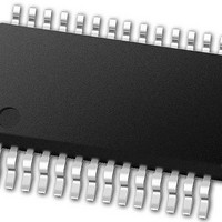
16-bit, 16 MIPS, 64KB Flash, 8KB RAM, Nanowatt XLP, USB OTG 28 SSOP .209in TUBE
Manufacturer
Microchip Technology
Specifications of PIC24FJ64GB002-I/SS
Processor Series
PIC24
Core
PIC24F
Data Bus Width
16 bit
Program Memory Type
Flash
Program Memory Size
64 KB
Data Ram Size
8192 B
Interface Type
I2C, SPI, UART
Maximum Clock Frequency
32 MHz
Number Of Programmable I/os
21
Number Of Timers
5
Operating Supply Voltage
2 V to 3.6 V
Maximum Operating Temperature
+ 85 C
Mounting Style
SMD/SMT
Package / Case
SSOP-28
Development Tools By Supplier
MPLAB Integrated Development Environment
Minimum Operating Temperature
- 40 C
Operating Temperature Range
- 40 C to + 85 C
Supply Current (max)
300 mA
Lead Free Status / Rohs Status
Lead free / RoHS Compliant
Available stocks
Company
Part Number
Manufacturer
Quantity
Price

Part Number:
PIC24FJ64GB002-I/SS
Manufacturer:
MICROCHIP/微芯
Quantity:
20 000


PIC24FJ64GB004 FAMILY
REGISTER 26-2:
DS39940D-page 282
bit 23
bit 15
bit 7
Legend:
R = Readable bit
-n = Value when device is unprogrammed
bit 23-16
bit 15
bit 14-12
bit 11
bit 10-8
bit 7-6
bit 5
FCKSM1
R/PO-1
R/PO-1
IESO
U-1
—
Unimplemented: Read as ‘1’
IESO: Internal External Switchover bit
1 = IESO mode (Two-Speed Start-up) is enabled
0 = IESO mode (Two-Speed Start-up) is disabled
PLLDIV<2:0>: USB 96 MHz PLL Prescaler Select bits
111 = Oscillator input divided by 12 (48 MHz input)
110 = Oscillator input divided by 8 (32 MHz input)
101 = Oscillator input divided by 6 (24 MHz input)
100 = Oscillator input divided by 5 (20 MHz input)
011 = Oscillator input divided by 4 (16 MHz input)
010 = Oscillator input divided by 3 (12 MHz input)
001 = Oscillator input divided by 2 (8 MHz input)
000 = Oscillator input used directly (4 MHz input)
PLL96MHZ: USB 96 MHz PLL Start-up Enable bit
1 = 96 MHz PLL is enabled automatically on start-up
0 = 96 MHz PLL is enabled by user in software (controlled with the PLLEN bit in CLKDIV<5>)
FNOSC<2:0>: Initial Oscillator Select bits
111 = Fast RC Oscillator with Postscaler (FRCDIV)
110 = Reserved
101 = Low-Power RC Oscillator (LPRC)
100 = Secondary Oscillator (SOSC)
011 = Primary Oscillator with PLL module (XTPLL, HSPLL, ECPLL)
010 = Primary Oscillator (XT, HS, EC)
001 = Fast RC Oscillator with Postscaler and PLL module (FRCPLL)
000 = Fast RC Oscillator (FRC)
FCKSM<1:0>: Clock Switching and Fail-Safe Clock Monitor Configuration bits
1x = Clock switching and Fail-Safe Clock Monitor are disabled
01 = Clock switching is enabled, Fail-Safe Clock Monitor is disabled
00 = Clock switching is enabled, Fail-Safe Clock Monitor is enabled
OSCIOFCN: OSCO Pin Configuration bit
If POSCMD<1:0> = 11 or 00:
1 = OSCO/CLKO/RA3 functions as CLKO (F
0 = OSCO/CLKO/RA3 functions as port I/O (RC15)
If POSCMD<1:0> = 10 or 01:
OSCIOFCN has no effect on OSCO/CLKO/RA3.
FCKSM0
PLLDIV2
R/PO-1
R/PO-1
U-1
—
CW2: FLASH CONFIGURATION WORD 2
PO = Program Once bit
OSCIOFCN
PLLDIV1
R/PO-1
R/PO-1
U-1
—
IOL1WAY
PLLDIV0
R/PO-1
R/PO-1
U-1
—
U = Unimplemented bit, read as ‘0’
‘1’ = Bit is set
OSC
PLL96MHZ
R/PO-1
/2)
U-1
U-1
—
—
FNOSC2
I2C1SEL
R/PO-1
R/PO-1
U-1
—
2010 Microchip Technology Inc.
‘0’ = Bit is cleared
POSCMD1
FNOSC1
R/PO-1
R/PO-1
U-1
—
POSCMD0
FNOSC0
R/PO-1
R/PO-1
U-1
—
bit 16
bit 8
bit 0
Related parts for PIC24FJ64GB002-I/SS
Image
Part Number
Description
Manufacturer
Datasheet
Request
R

Part Number:
Description:
Manufacturer:
Microchip Technology Inc.
Datasheet:
Part Number:
Description:
Manufacturer:
Microchip Technology Inc.
Datasheet:
Part Number:
Description:
Manufacturer:
Microchip Technology Inc.
Datasheet:
Part Number:
Description:
Manufacturer:
Microchip Technology Inc.
Datasheet:
Part Number:
Description:
Manufacturer:
Microchip Technology Inc.
Datasheet:
Part Number:
Description:
Manufacturer:
Microchip Technology Inc.
Datasheet:
Part Number:
Description:
Manufacturer:
Microchip Technology Inc.
Datasheet:
Part Number:
Description:
Manufacturer:
Microchip Technology Inc.
Datasheet: