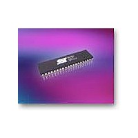
SST89E58RD2-40-I-TQJE Microchip Technology, SST89E58RD2-40-I-TQJE Datasheet - Page 45

SST89E58RD2-40-I-TQJE
Manufacturer Part Number
SST89E58RD2-40-I-TQJE
Description
4.5 To 5.5V FlashFlex 8-bit 8051 Microcontroller 44 TQFP 10x10x1mm TRAY
Manufacturer
Microchip Technology
Series
FlashFlex®r
Specifications of SST89E58RD2-40-I-TQJE
Core Processor
8051
Core Size
8-Bit
Speed
40MHz
Connectivity
EBI/EMI, SPI, UART/USART
Peripherals
Brown-out Detect/Reset, POR, WDT
Number Of I /o
36
Program Memory Size
32KB (32K x 8)
Program Memory Type
FLASH
Eeprom Size
8K x 8
Ram Size
1K x 8
Voltage - Supply (vcc/vdd)
4.5 V ~ 5.5 V
Oscillator Type
External
Operating Temperature
-40°C ~ 85°C
Package / Case
44-TQFP
Processor Series
FlashFlex51
Core
C51
Data Bus Width
8 bit
Data Ram Size
1 KB
Interface Type
SPI
Maximum Clock Frequency
40 MHz
Number Of Programmable I/os
5
Number Of Timers
3
Operating Supply Voltage
4.5 V to 5.5 V
Maximum Operating Temperature
+ 85 C
Mounting Style
SMD/SMT
Minimum Operating Temperature
- 40 C
Lead Free Status / RoHS Status
Lead free / RoHS Compliant
Data Converters
-
Lead Free Status / Rohs Status
Details
Available stocks
Company
Part Number
Manufacturer
Quantity
Price
Company:
Part Number:
SST89E58RD2-40-I-TQJE
Manufacturer:
Microchip Technology
Quantity:
10 000
Part Number:
SST89E58RD2-40-I-TQJE
Manufacturer:
SST
Quantity:
20 000
FlashFlex MCU
SST89E54RD2A/RDA / SST89E58RD2A/RDA
The user could use the possible addresses above to select
slave 3 only. Another combination could be to select slave 2
and 3 only as shown below.
More than one slave may have the same SADDR address
as well, and a given address could be used to modify the
address so that it is unique.
6.1.2.2 Using the Broadcast Address to Select Slaves
Using the broadcast address, the master can communicate
with all the slaves at once. It is formed by performing a logi-
cal OR of SADDR and SADEN with ‘0’s in the result treated
as “don’t cares”.
“Don’t cares” allow for a wider range in defining the broad-
cast address, but in most cases, the broadcast address will
be FFH.
On reset, SADDR and SADEN are “0”. This produces an
given address of all “don’t cares” as well as a broadcast
address of all “don’t cares.” This effectively disables Auto-
matic Addressing mode and allows the microcontroller to
function as a standard 8051, which does not make use of
this feature.
©2008 Silicon Storage Technology, Inc.
Slaves 2 and 3
FIGURE
Select Slaves 2 and 3 Only
6-4: SPI Master-slave Interconnection
Slave 1
1111 0001
+1111 1010 = SADEN
1111 1X11
Clock Generator
SPI
= SADDR
= Broadcast
Possible Addresses
MSB Master LSB
8-bit Shift Register
1111 0011
45
SCK
SS#
MISO MISO
MOSI MOSI
V
6.2 Serial Peripheral Interface
6.2.1 SPI Features
•
•
•
•
•
•
•
6.2.2 SPI Description
The serial peripheral interface (SPI) allows high-speed syn-
chronous data transfer between the SST89E/V5xRDxA
and peripheral devices or between several SST89E/
V5xRDxA devices.
Figure 6-4 shows the correspondence between master
and slave SPI devices. The SCK pin is the clock output and
input for the master and slave modes, respectively. The SPI
clock generator will start following a write to the master
devices SPI data register. The written data is then shifted
out of the MOSI pin on the master device into the MOSI pin
of the slave device. Following a complete transmission of
one byte of data, the SPI clock generator is stopped and
the SPIF flag is set. An SPI interrupt request will be gener-
ated if the SPI Interrupt Enable bit (SPIE) and the Serial
Port Interrupt Enable bit (ES) are both set.
An external master drives the Slave Select input pin, SS#/
P1[4], low to select the SPI module as a slave. If SS#/P1[4]
has not been driven low, then the slave SPI unit is not
active and the MOSI/P1[5] port can also be used as an
input port pin.
CPHA and CPOL control the phase and polarity of the SPI
clock. Figures 6-5 and 6-6 show the four possible combina-
tions of these two bits.
DD
Master or slave operation
10 MHz bit frequency (max)
LSB first or MSB first data transfer
Four programmable bit rates
End of transmission (SPIF)
Write collision flag protection (WCOL)
Wake up from idle mode (slave mode only)
V
SCK
SS#
SS
MSB Slave LSB
8-bit Shift Register
1339 F19.0
S71339-02-000
Data Sheet
02/08


