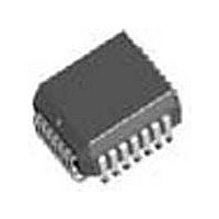
TP3403VNOPB National Semiconductor, TP3403VNOPB Datasheet - Page 3

TP3403VNOPB
Manufacturer Part Number
TP3403VNOPB
Description
Manufacturer
National Semiconductor
Datasheet
1.TP3403VNOPB.pdf
(16 pages)
Specifications of TP3403VNOPB
Operating Supply Voltage (typ)
5V
Operating Supply Voltage (min)
4.75V
Operating Supply Voltage (max)
5.25V
Operating Temp Range
0C to 70C
Operating Temperature Classification
Commercial
Package Type
PLCC
Mounting
Surface Mount
Pin Count
28
Lead Free Status / RoHS Status
Compliant
Pin Descriptions
CI
CO
CCLK
CS
INT
L
L
Functional Description
POWER-UP POWER-DOWN CONTROL
Following the initial application of power the DASL enters
the power-down (de-activated) state in which all the internal
circuits are inactive and in a low power state except for the
line-signal detect circuit and the necessary bias circuit the
line output L
outputs are inactive All bits in the Control Register power-
up initially set to ‘0’ so that the device always initializes as
the Master end Thus at the Slave end a control word must
be written through the MICROWIRE port to select Slave
mode While powered-down the Line-Signal Detect circuits
in both Master and Slave devices continually monitor the
line to enable loop transmission to be initiated from either
end
To power-up the device and initiate activation bit C6 in the
Control Register must be set high Setting C6 low de-acti-
vates the loop and powers-down the device see Table I
o
i
Don’t Care
MBS FS
at Master
Pin I P
Name
4 kHz
Open
c
o
MICROWIRE control channel serial data in-
put
MICROWIRE control channel serial data out-
put
Clock input for the MICROWIRE control
channel
Chip Select input which enables the MICRO-
WIRE control channel data to be shifted in
and out when pulled low When high this pin
inhibits the MICROWIRE interface
Interrupt output a latched output signal
which is normally high-impedance and goes
low to indicate a change of status of the loop
transmission system This latch is cleared
when the Status Register is read by the mi-
croprocessor
Transmit AMI signal output to the line trans-
former This pin is capable of driving a load
impedance
Receive AMI signal input from the line trans-
former This is a high impedance input
TABLE I Master Mode Burst
Sync Control (TP3401 Only)
is in a low impedance state and all digital
State
C6
0
1
1
Powered-down Line-Signal
Detect active
Powered-up sending bursts
synchronized to FS
Powered-up sending bursts
synchronized to MBS
t
(Continued)
60
Description
Action
a
3
Figure 3 shows the pulse shape at the L
LINE TRANSMIT SECTION
Alternate Mark Inversion (AMI) line coding is used on the
DASL because of its spectral efficiency and null dc energy
content All transmitted bits excluding the start bit are
scrambled by a 9-bit scrambler to provide good spectral
spreading with a strong timing content The scrambler feed-
back polynomial is
Pulse shaping is obtained by means of a raised cosine
switched-capacitor filter in order to limit rf energy and
crosstalk while minimizing inter-symbol interference (isi)
template for the typical power spectrum transmitted to the
line with random data is shown in Figure 4
The line-driver output L
through a capacitor and termination resistor A 1 1 trans-
former terminated in 100
typically 1 3V pk-pk on the line Over-voltage protection
must be included in the interface circuit
LINE RECEIVE SECTION
The front-end of the receive section consists of a continu-
ous anti-alias filter followed by a switched-capacitor low-
pass filter designed to limit the noise bandwidth with mini-
mum intersymbol interference To correct pulse attenuation
and distortion caused by the transmission line an AGC cir-
cuit and first-order equalizer adapt to the received pulse
shape thus restoring a ‘‘flat’’ channel response with maxi-
mum received eye opening over a wide spread of cable
attenuation characteristics
From the equalized output a DPLL (Digital Phase-Locked
Loop) recovers a low-jitter clock for optimum sampling of
the received symbols The MCLK input provides the refer-
ence clock for the DPLL at 2 048 MHz At the Master end of
the loop this reference is the network clock (BCLK) which
controls all transmit functions the DPLL clock is used only
for received data sampling At the Slave end however a
2 048 MHz crystal is required to generate a stable local os-
cillator which is used as a reference by the DPLL to run both
the receive and transmit sides of the DASL device
Following detection of the recovered symbols the received
data is de-scrambled by the same x
and presented to the digital system interface circuit
When the device is de-activated a Line-Signal Detect circuit
remains powered-up to detect the presence of incoming
bursts if the far-end starts to activate the loop From a
‘‘cold’’ start acquisition of bit timing and equalizer conver-
gence with random scrambled data takes approximately
25 ms at each end of the loop Full loop burst synchroniza-
tion is achieved approximately 50 ms after the ‘‘activate’’
command at the originating end
x
o
9
a
is designed to drive a transformer
results in a signal amplitude of
x
5
a
1
9
a
x
o
5
a
output while a
1 polynomial


