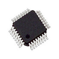
MC33911G5ACR2 Freescale, MC33911G5ACR2 Datasheet - Page 86

MC33911G5ACR2
Manufacturer Part Number
MC33911G5ACR2
Description
Manufacturer
Freescale
Datasheet
1.MC33911G5ACR2.pdf
(92 pages)
Specifications of MC33911G5ACR2
Turn Off Delay Time
10us
Number Of Drivers
2
Operating Temperature (min)
-40C
Operating Temperature (max)
125C
Operating Temperature Classification
Automotive
Lead Free Status / RoHS Status
Compliant
Available stocks
Company
Part Number
Manufacturer
Quantity
Price
Company:
Part Number:
MC33911G5ACR2
Manufacturer:
Freescale Semiconductor
Quantity:
10 000
WDERR - Watchdog Error
watchdog resistor. In this condition the watchdog is using the
internal, lower precision timebase. The Windowing function is
disabled.
WDOFF - Watchdog Off
to Ground and therefore disabled. In this case watchdog
timeouts are disabled and the device automatically enters
Normal mode out of Reset. This might be necessary for
software debugging and for programming the Flash memory.
WDWO - Watchdog Window Open
open for clears. The purpose of this bit is for testing. Should
be ignored in case WDERR is High.
Analog Multiplexer Control Register - MUXCR
the divider ration for the Lx input divider.
LXDS - Lx Analog Input Divider Select
analog inputs. Voltage is internally clamped to VDD.
Analog Integrated Circuit Device Data
Freescale Semiconductor
This read-only bit signals the detection of a missing
1 = WDCONF pin resistor missing
0 = WDCONF pin resistor not floating
This read-only bit signals that the watchdog pin connected
1 = Watchdog is disabled
0 = Watchdog is enabled
This read-only bit signals when the watchdog window is
1 = Watchdog window open
0 = Watchdog window closed
This register controls the analog multiplexer and selects
This write-only bit selects the resistor divider for the Lx
0 = Lx Analog divider: 1
1 = Lx Analog divider: 3.6 (typ.)
Table 57. Analog Multiplexer Control Register -$C
Condition
Reset
Reset
Value
Write
LXDS
POR
C3
1
POR, Reset mode or ext_reset
MX2
C2
0
MX1
C1
0
MX0
C0
0
MXx - Analog Multiplexer Input Select
multiplexed to the ADOUT0 pin according to
buffer is not powered and the ADOUT0 output is left floating
to achieve lower current consumption.
Table 58.
Configuration Register - CFR
CYSX8 - Cyclic Sense Timing x 8.
shown in
MX2
These write-only bits selects which analog input is
When disabled or when in Stop or Sleep mode, the output
This register controls the cyclic sense timing multiplier.
This write-only bit influences the cyclic sense period as
1 = Multiplier enabled
0 = None
Table 59. Configuration Register - $D
0
0
0
0
1
1
1
1
Condition
Reset
Value
Reset
Write
Table
Analog Multiplexer Channel Select
MX1
0
0
1
1
0
0
1
1
POR, Reset
ext_reset
mode or
55.
C3
0
0
MX0
0
1
0
1
0
1
0
1
LOGIC COMMANDS AND REGISTERS
FUNCTIONAL DEVICE OPERATIONS
CYSX8
POR
C2
0
Die Temperature Sensor
VSENSE input
POR
C1
Reserved
Reserved
Reserved
0
0
Meaning
Disabled
L1 input
L2 input
Table
POR
C0
0
0
58.
33911
86


