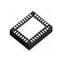
DS90LV804TSQ National Semiconductor, DS90LV804TSQ Datasheet - Page 4

DS90LV804TSQ
Manufacturer Part Number
DS90LV804TSQ
Description
Manufacturer
National Semiconductor
Datasheet
1.DS90LV804TSQ.pdf
(10 pages)
Specifications of DS90LV804TSQ
Number Of Elements
4
Input Type
CMOS/TTL
Operating Supply Voltage (typ)
3.3V
Differential Input High Threshold Voltage
100mV
Diff. Input Low Threshold Volt
-100mV
Output Type
Repeater
Differential Output Voltage
600mV
Transmission Data Rate
800Mbps
Propagation Delay Time
3.2ns
Operating Temp Range
-40C to 85C
Operating Temperature Classification
Industrial
Mounting
Surface Mount
Pin Count
32
Number Of Receivers
4
Number Of Drivers
4
Lead Free Status / RoHS Status
Not Compliant
Available stocks
Company
Part Number
Manufacturer
Quantity
Price
Part Number:
DS90LV804TSQ
Manufacturer:
NS/国半
Quantity:
20 000
Company:
Part Number:
DS90LV804TSQ/NOPB
Manufacturer:
FREE
Quantity:
840
Company:
Part Number:
DS90LV804TSQE/NOPB
Manufacturer:
TI/NSC
Quantity:
8 322
Company:
Part Number:
DS90LV804TSQX/NOPB
Manufacturer:
TI/NSC
Quantity:
8 322
www.national.com
LVTTL DC SPECIFICATIONS (EN)
V
V
I
I
C
V
LVDS INPUT DC SPECIFICATIONS (INn±)
V
V
V
V
C
I
IH
IL
IN
Symbol
IH
IL
CL
TH
TL
ID
CMR
IN1
IN2
Absolute Maximum Ratings
Electrical Characteristics
Over recommended operating supply and temperature ranges unless other specified.
Supply Voltage (V
CMOS Input Voltage (EN)
LVDS Input Voltage (Note 4)
LVDS Output Voltage
LVDS Output Short Circuit Current
Junction Temperature
Storage Temperature
Lead Temperature (Solder, 4sec)
Max Pkg Power Capacity @ 25°C
Thermal Resistance
θ
θ
Package Derating above +25°C
ESD Last Passing Voltage (LVDS output pins)
JA
JC
HBM, 1.5kΩ, 100pF
EIAJ, 0Ω, 200pF
Charged Device Model
High Level Input Voltage
Low Level Input Voltage
High Level Input Current
Low Level Input Current
Input Capacitance
Input Clamp Voltage
Differential Input High Threshold
(Note 6)
Differential Input Low Threshold
(Note 6)
Differential Input Voltage
Common Mode Voltage Range
Input Capacitance
Input Current
DD
Parameter
)
−0.3V to (V
−0.3V to (V
−0.3V to (V
−65°C to +150°C
V
V
Any Digital Input Pin to V
I
V
V
V
V
V
V
IN+ or IN− to V
V
V
CL
IN
IN
CM
DD
CM
DD
CM
ID
IN
IN
−0.3V to +4.0V
= −18 mA
= V
= V
= 150 mV, V
= 3.45V, V
= 0V, V
= 3.45V
= 3.45V
(Note 3)
= 0.8V to 3.4V,
= 0.8V to 3.4V,
= 0.8V to 3.4V, V
33.3mW/°C
29.5°C/W
DD
SS
DD
DD
DD
3.5°C/W
+90 mA
+150°C
, V
+0.3V)
+0.3V)
+0.3V)
= V
4.16W
1000V
260°C
12 kV
DD
250V
DD
DDMAX
= V
DD
SS
= V
DD
= V
DDMAX
DDMAX
Conditions
= 3.45V
4
DDMAX
DD
= 3.45V
SS
Recommended Operating
Conditions
Note 3: Absolute maximum ratings are those values beyond which damage
to the device may occur. The databook specifications should be met, without
exception, to ensure that the system design is reliable over its power supply,
temperature, and output/input loading variables. National does not
recommend operation of products outside of recommended operation
conditions.
Note 4: V
ESD Last Passing Voltage (All other pins)
Supply Voltage (V
Input Voltage (V
Output Voltage (V
Operating Temperature (T
HBM, 1.5kΩ, 100pF
EIAJ, 0Ω, 200pF
Charged Device Model
Industrial
ID
max < 2.4V
I
) (Note 4)
O
CC
)
)
A
GND
−100
)
−1.5
0.05
Min
−10
−10
100
−10
−10
2.0
(Note 5)
−0.8
Typ
3.5
3.5
0
0
−40°C to +85°C
3.15V to 3.45V
2400
Max
3.40
V
+10
+10
+10
+10
100
0.8
DD
0V to V
0V to V
1000V
250V
8 kV
Units
mV
mV
mV
µA
µA
µA
µA
pF
pF
DD
DD
V
V
V
V


