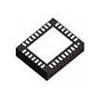
DS90LV804TSQ National Semiconductor, DS90LV804TSQ Datasheet - Page 8

DS90LV804TSQ
Manufacturer Part Number
DS90LV804TSQ
Description
Manufacturer
National Semiconductor
Datasheet
1.DS90LV804TSQ.pdf
(10 pages)
Specifications of DS90LV804TSQ
Number Of Elements
4
Input Type
CMOS/TTL
Operating Supply Voltage (typ)
3.3V
Differential Input High Threshold Voltage
100mV
Diff. Input Low Threshold Volt
-100mV
Output Type
Repeater
Differential Output Voltage
600mV
Transmission Data Rate
800Mbps
Propagation Delay Time
3.2ns
Operating Temp Range
-40C to 85C
Operating Temperature Classification
Industrial
Mounting
Surface Mount
Pin Count
32
Number Of Receivers
4
Number Of Drivers
4
Lead Free Status / RoHS Status
Not Compliant
Available stocks
Company
Part Number
Manufacturer
Quantity
Price
Part Number:
DS90LV804TSQ
Manufacturer:
NS/国半
Quantity:
20 000
Company:
Part Number:
DS90LV804TSQ/NOPB
Manufacturer:
FREE
Quantity:
840
Company:
Part Number:
DS90LV804TSQE/NOPB
Manufacturer:
TI/NSC
Quantity:
8 322
Company:
Part Number:
DS90LV804TSQX/NOPB
Manufacturer:
TI/NSC
Quantity:
8 322
www.national.com
OUTPUT INTERFACING
The DS90LV804 outputs signals that are compliant to the
LVDS standard. Their outputs can be DC-coupled to most
common differential receivers. The following figure illustrates
typical DC-coupled interface to common differential receivers
Typical Performance
Characteristics
Dynamic power supply current was measured while running a clock or PRBS
2
V
23
CM
-1 pattern with all 4 channels active. V
= 1.2V
Power Supply Current vs. Bit Data Rate
Typical DS90LV804 Output DC-Coupled Interface to an LVDS, CML or LVPECL Receiver
CC
= 3.3V, T
A
= +25°C, V
20156741
ID
= 0.5V,
8
and assumes that the receivers have high impedance inputs.
While most differential receivers have a common mode input
range that can accommodate LVDS compliant signals, it is
recommended to check respective receiver's data sheet prior
to implementing the suggested interface implementation.
Packaging Information
The Leadless Leadframe Package (LLP) is a leadframe
based chip scale package (CSP) that may enhance chip
speed, reduce thermal impedance, and reduce the printed
circuit board area required for mounting. The small size and
very low profile make this package ideal for high density PCBs
used in small-scale electronic applications such as cellular
phones, pagers, and handheld PDAs. The LLP package is
offered in the no Pullback configuration. In the no Pullback
configuration the standard solder pads extend and terminate
at the edge of the package. This feature offers a visible solder
fillet after board mounting.
The LLP has the following advantages:
•
•
•
•
•
For more details about LLP packaging technology, refer to
applications note AN-1187, "Leadless Leadframe Package"
Low thermal resistance
Reduced electrical parasitics
Improved board space efficiency
Reduced package height
Reduced package mass
20156734


