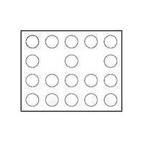
IP3337CX18/LF/P,13 NXP Semiconductors, IP3337CX18/LF/P,13 Datasheet

IP3337CX18/LF/P,13
Specifications of IP3337CX18/LF/P,13
Related parts for IP3337CX18/LF/P,13
IP3337CX18/LF/P,13 Summary of contents
Page 1
IP3337CX18 7-channel integrated LC-filter network with ESD input protection to IEC 61000-4-2 level 4 Rev. 02 — 10 March 2009 1. Product profile 1.1 General description The IP3337CX18 is a 7-channel RF signals in the 800 MHz to 3000 MHz ...
Page 2
... NXP Semiconductors 2. Pinning information 2.1 Pinning Fig 1. Table 1. Pin A2 and A5 A1 and A4 B1 and B5 C2 and C5 C1 and C4 D2 and D5 D1 and D4 A3, B3, C3 and B4 3. Ordering information Table 2. Ordering information Type number Package Name IP3337CX18/LF WLCSP18 IP3337CX18_2 Product data sheet 7-channel integrated LC-fi ...
Page 3
... NXP Semiconductors 4. Functional diagram Fig 2. 5. Limiting values Table 3. In accordance with the Absolute Maximum Rating System (IEC 60134). Symbol ESD ch( tot T stg T reflow(peak) T amb [1] Device tested with 1000 pulses contact discharges, according to the IEC 61000-4-2 model, which far exceeds IEC 61000-4-2, level contact discharge). ...
Page 4
... NXP Semiconductors 6. Characteristics Table unless otherwise specified. amb Symbol Parameter R s(ch s(ch [1] Guaranteed by design. Table unless otherwise specified. amb Symbol Parameter il f 3dB ct 7. Application information 7.1 Insertion loss The setup for measuring insertion loss Fig 3. The measured frequency response curves for all channels are shown in ...
Page 5
... NXP Semiconductors (dB) (1) Channel 2 (pins A1 and A4). (2) Channel 5 (pins C1 and C4). (3) Channel 7 (pins D1 and D4). Fig 4. 7.2 Crosstalk The setup for measuring crosstalk Fig 5. The crosstalk between adjacent channels within the IP3337CX18 for different channel pairs measured cases, all unused connections are terminated with 50 ...
Page 6
... NXP Semiconductors ct (1) Channels 2 and 5 (pins A1 and C4). (2) Channels 3 and 4 (pins B1 and C5). (3) Channels 3 and 6 (pins B1 and D5). (4) Channels 2 and 1 (pins A1 and A5). Fig 6. IP3337CX18_2 Product data sheet 7-channel integrated LC-filter network with ESD input protection Measured crosstalk between adjacent channels Rev. 02 — 10 March 2009 ...
Page 7
... NXP Semiconductors 8. Package outline WLCSP18: wafer level chip-size package; 18 bumps; 2.06 x 1.66 x 0.61 mm bump A1 index Dimensions Unit max 0.66 0.22 0.31 mm nom 0.61 0.20 0.41 0.26 min 0.56 0.18 0.21 Outline version IEC IP3337CX18/LF Fig 7. Package outline IP3337CX18/LF (WLCSP18) IP3337CX18_2 Product data sheet 7-channel integrated LC-fi ...
Page 8
... NXP Semiconductors 9. Soldering of WLCSP packages 9.1 Introduction to soldering WLCSP packages This text provides a very brief insight into a complex technology. A more in-depth account of soldering WLCSP (Wafer Level Chip-Size Packages) can be found in application note AN10439 “Wafer Level Chip Scale Package” and in application note AN10365 “Surface mount refl ...
Page 9
... NXP Semiconductors Fig 8. For further information on temperature profiles, refer to application note AN10365 “Surface mount reflow soldering description” . 9.3.1 Stand off The stand off between the substrate and the chip is determined by: • The amount of printed solder on the substrate • The size of the solder land on the substrate • ...
Page 10
... NXP Semiconductors Device removal can be done when the substrate is heated until it is certain that all solder joints are molten. The chip can then be carefully removed from the substrate without damaging the tracks and solder lands on the substrate. Removing the device must be done using plastic tweezers, because metal tweezers can damage the silicon. The surface of the substrate should be carefully cleaned and all solder and fl ...
Page 11
... Right to make changes — NXP Semiconductors reserves the right to make changes to information published in this document, including without limitation specifications and product descriptions, at any time and without notice ...
Page 12
... NXP Semiconductors 14. Contents 1 Product profi 1.1 General description 1.2 Features . . . . . . . . . . . . . . . . . . . . . . . . . . . . . . 1 1.3 Applications . . . . . . . . . . . . . . . . . . . . . . . . . . . 1 2 Pinning information . . . . . . . . . . . . . . . . . . . . . . 2 2.1 Pinning . . . . . . . . . . . . . . . . . . . . . . . . . . . . . . . 2 3 Ordering information . . . . . . . . . . . . . . . . . . . . . 2 4 Functional diagram . . . . . . . . . . . . . . . . . . . . . . 3 5 Limiting values Characteristics . . . . . . . . . . . . . . . . . . . . . . . . . . 4 7 Application information 7.1 Insertion loss . . . . . . . . . . . . . . . . . . . . . . . . . . 4 7.2 Crosstalk Package outline . . . . . . . . . . . . . . . . . . . . . . . . . 7 9 Soldering of WLCSP packages ...


