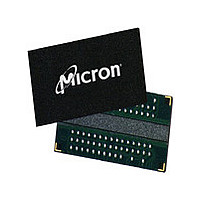
MT47H128M16HG-3 IT:A Micron Technology Inc, MT47H128M16HG-3 IT:A Datasheet - Page 111

MT47H128M16HG-3 IT:A
Manufacturer Part Number
MT47H128M16HG-3 IT:A
Description
Manufacturer
Micron Technology Inc
Type
DDR2 SDRAMr
Datasheet
1.MT47H128M16HG-3_ITA.pdf
(134 pages)
Specifications of MT47H128M16HG-3 IT:A
Organization
128Mx16
Address Bus
17b
Access Time (max)
4.5ns
Maximum Clock Rate
667MHz
Operating Supply Voltage (typ)
1.8V
Package Type
FBGA
Operating Temp Range
-40C to 85C
Operating Supply Voltage (max)
1.9V
Operating Supply Voltage (min)
1.7V
Supply Current
275mA
Pin Count
84
Mounting
Surface Mount
Operating Temperature Classification
Industrial
Lead Free Status / RoHS Status
Compliant
- Current page: 111 of 134
- Download datasheet (10Mb)
Figure 64: Bank Write – Without Auto Precharge
PDF: 09005aef824f87b6
2gbddr2.pdf – Rev. F 12/10 EN
Bank select
DQS, DQS#
Command
Address
DQ 6
CK#
CKE
A10
DM
CK
NOP 1
T0
Notes:
Bank x
ACT
RA
RA
T1
1. NOP commands are shown for ease of illustration; other commands may be valid at
2. BL = 4 and AL = 0 in the case shown.
3. Disable auto precharge.
4. “Don’t Care” if A10 is HIGH at T9.
5. Subsequent rising DQS signals must align to the clock within
6. DI n = data-in for column n; subsequent elements are applied in the programmed order.
7.
8.
t CK
these times.
t
t
DSH is applicable during
DSS is applicable during
t RCD
NOP 1
T2
t CH
t CL
WRITE 2
Bank x
Col n
3
T3
WL ± t DQSS (NOM)
WL = 2
NOP 1
t
111
T4
t
DQSS (MAX) and is referenced from CK T6 or T7.
DQSS (MIN) and is referenced from CK T5 or T6.
t WPRE
NOP 1
T5
Micron Technology, Inc. reserves the right to change products or specifications without notice.
DI
n
T5n
t DQSL t DQSH t WPST
t RAS
2Gb: x4, x8, x16 DDR2 SDRAM
NOP 1
5
T6
T6n
Transitioning Data
NOP 1
T7
© 2006 Micron Technology, Inc. All rights reserved.
t
DQSS.
t WR
NOP 1
T8
One bank
All banks
Don’t Care
Bank x 4
T9
PRE
WRITE
t RP
Related parts for MT47H128M16HG-3 IT:A
Image
Part Number
Description
Manufacturer
Datasheet
Request
R

Part Number:
Description:
IC SDRAM 64MBIT 133MHZ 54TSOP
Manufacturer:
Micron Technology Inc
Datasheet:

Part Number:
Description:
IC SDRAM 64MBIT 5.5NS 86TSOP
Manufacturer:
Micron Technology Inc
Datasheet:

Part Number:
Description:
IC SDRAM 64MBIT 200MHZ 86TSOP
Manufacturer:
Micron Technology Inc
Datasheet:

Part Number:
Description:
IC SDRAM 64MBIT 133MHZ 54TSOP
Manufacturer:
Micron Technology Inc
Datasheet:

Part Number:
Description:
IC SDRAM 128MBIT 133MHZ 54TSOP
Manufacturer:
Micron Technology Inc
Datasheet:

Part Number:
Description:
IC SDRAM 256MBIT 133MHZ 90VFBGA
Manufacturer:
Micron Technology Inc
Datasheet:

Part Number:
Description:
IC SDRAM 128MBIT 133MHZ 54TSOP
Manufacturer:
Micron Technology Inc
Datasheet:

Part Number:
Description:
IC SDRAM 256MBIT 133MHZ 54TSOP
Manufacturer:
Micron Technology Inc
Datasheet:

Part Number:
Description:
IC DDR SDRAM 512MBIT 6NS 66TSOP
Manufacturer:
Micron Technology Inc
Datasheet:

Part Number:
Description:
IC SDRAM 128MBIT 167MHZ 86TSOP
Manufacturer:
Micron Technology Inc
Datasheet:

Part Number:
Description:
IC SDRAM 128MBIT 143MHZ 86TSOP
Manufacturer:
Micron Technology Inc
Datasheet:

Part Number:
Description:
SDRAM 256M-BIT 1.8V 54-PIN VFBGA
Manufacturer:
Micron Technology Inc
Datasheet:

Part Number:
Description:
IC SDRAM 128MBIT 143MHZ 86TSOP
Manufacturer:
Micron Technology Inc
Datasheet:

Part Number:
Description:
IC SDRAM 128MBIT 125MHZ 54VFBGA
Manufacturer:
Micron Technology Inc
Datasheet:

Part Number:
Description:
IC SDRAM 128MBIT 125MHZ 54VFBGA
Manufacturer:
Micron Technology Inc
Datasheet:


