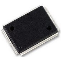
MT48LC2M32B2P-6:G Micron Technology Inc, MT48LC2M32B2P-6:G Datasheet - Page 16

MT48LC2M32B2P-6:G
Manufacturer Part Number
MT48LC2M32B2P-6:G
Description
IC, SDRAM, 64MBIT, 166MHZ, TSOP-86
Manufacturer
Micron Technology Inc
Type
SDRAMr
Series
-r
Specifications of MT48LC2M32B2P-6:G
Organization
2Mx32
Density
64Mb
Address Bus
13b
Access Time (max)
17/7.5/5.5ns
Maximum Clock Rate
166MHz
Operating Supply Voltage (typ)
3.3V
Package Type
TSOP-II
Operating Temp Range
0C to 70C
Operating Supply Voltage (max)
3.6V
Operating Supply Voltage (min)
3V
Supply Current
180mA
Pin Count
86
Mounting
Surface Mount
Operating Temperature Classification
Commercial
Memory Type
DRAM - Sychronous
Access Time
5.5ns
Page Size
64Mbit
Memory Case Style
TSOP
No. Of Pins
86
Operating Temperature Range
0°C To +70°C
Frequency
166MHz
Supply Voltage
3.3V
Format - Memory
RAM
Memory Size
64M (2Mx32)
Speed
167MHz
Interface
Parallel
Voltage - Supply
3 V ~ 3.6 V
Operating Temperature
0°C ~ 70°C
Package / Case
86-TFSOP (0.400", 10.16mm Width)
Filter Terminals
SMD
Rohs Compliant
Yes
Lead Free Status / RoHS Status
Compliant
Lead Free Status / RoHS Status
Compliant, Lead free / RoHS Compliant
Available stocks
Company
Part Number
Manufacturer
Quantity
Price
Part Number:
MT48LC2M32B2P-6:G
Manufacturer:
MICRON
Quantity:
20 000
Figure 7:
Table 6:
Operating Mode
Write Burst Mode
PDF: 09005aef80725c0b/Source: 09005aef806fc13c
64MSDRAM_2.fm - Rev. M 10/07 EN
CAS Latency
CAS Latency
Reserved states should not be used as unknown operation or incompatibility with future
versions may result.
COMMAND
COMMAND
The normal operating mode is selected by setting M7 and M8 to zero; the other combi-
nations of values for M7 and M8 are reserved for future use and/or test modes. The
programmed burst length applies to both read and write bursts.
Test modes and reserved states should not be used because unknown operation or
incompatibility with future versions may result.
When M9 = 0, the burst length programmed via M0–M2 applies to both read and write
bursts; when M9 = 1, the programmed burst length applies to read bursts, but write
accesses are single-location (nonburst) accesses.
CLK
CLK
DQ
DQ
Speed
-7E
-75
-6
READ
READ
T0
T0
CL = 2
NOP
NOP
T1
T1
t
t AC
LZ
16
CL = 3
NOP
T2
Micron Technology, Inc., reserves the right to change products or specifications without notice.
T2
NOP
Allowable Operating Frequency (MHz)
t
t AC
D
LZ
t OH
CL = 2
OUT
≤133
≤100
–
T3
T3
NOP
D
t OH
OUT
64Mb: x4, x8, x16 SDRAM
DON’T CARE
UNDEFINED
Functional Description
©2000 Micron Technology, Inc. All rights reserved.
T4
CL = 3
≤166
≤143
≤133


