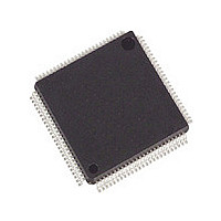
ADV7400AKSTZ-80 Analog Devices Inc, ADV7400AKSTZ-80 Datasheet - Page 3

ADV7400AKSTZ-80
Manufacturer Part Number
ADV7400AKSTZ-80
Description
Manufacturer
Analog Devices Inc
Datasheet
1.ADV7400AKSTZ-80.pdf
(16 pages)
Specifications of ADV7400AKSTZ-80
Lead Free Status / RoHS Status
Compliant
Available stocks
Company
Part Number
Manufacturer
Quantity
Price
Company:
Part Number:
ADV7400AKSTZ-80
Manufacturer:
ADI
Quantity:
303
Part Number:
ADV7400AKSTZ-80
Manufacturer:
ADI/亚德诺
Quantity:
20 000
ELECTRICAL CHARACTERISTICS
A
temperature range, unless otherwise noted.
Table 1. Electrical Characteristics
Parameter
STATIC PERFORMANCE
DIGITAL INPUTS
DIGITAL OUTPUTS
POWER REQUIREMENTS
1
2
3
4
5
6
7
The min/max specifications are guaranteed over this range.
Temperature range T
All ADC linearity tests performed at input range of full scale are −12.5%, and at zero scale they are +12.5%.
Specifications for the ADV7400AKSTZ-110 and the ADV7400ABSTZ-110 only.
Pins: 1, 2, 3, 13, 14, 16, 19, 24, 29, 30, 31, 32, 33, 34, 35, 45, 79, 83, 84, 87, 88, 95, 96, 97, 100.
Guaranteed by characterization.
Pins: 45, 34, 33, 32, 31, 30, 29, 24, 14, 13 (P20 to P29).
VDD
Resolution (each ADC)
Integral Nonlinearity
Integral Nonlinearity
Integral Nonlinearity
Integral Nonlinearity
Differential Nonlinearity
Differential Nonlinearity
Differential Nonlinearity
Differential Nonlinearity
Input High Voltage
Input Low Voltage
XTAL High Voltage
XTAL Low Voltage
Input High Voltage
Input Low Voltage
Input Current
Input Capacitance
Output High Voltage
Output Low Voltage
High Impedance Leakage Current
Output Capacitance
Digital Core Power Supply
Digital I/O Power Supply
PLL Power Supply
Analog Power Supply
Digital Core Supply Current
Digital I/O Supply Current
PLL Supply Current
Analog Supply Current
Power-Down Current
Green Mode Power-Down
Power-Up Time
= 3.15 V to 3.45 V, D
MIN
6
to T
6
3
6
MAX
VDD
: −40°C to +85°C.
= 1.65 V to 2.0 V, D
1 , 2
Symbol
N
INL
INL
INL
INL
DNL
DNL
DNL
DNL
V
V
V
V
V
V
I
C
V
V
I
C
D
D
P
A
I
I
I
I
I
I
T
IN
LEAK
DVDD
DVDDIO
PVDD
AVDD
PWRDN
PWRDNG
VDD
PWRUP
IH
IL
IH
IL
IH
IL
IN
OH
OL
OUT
VDD
VDD
VDDIO
VDDIO
Test Conditions
BSL at 27 MHz (at a 10-bit level)
BSL at 54 MHz (at a 10-bit level)
BSL at 74 MHz (at a 10-bit level)
BSL at 110 MHz (at an 8-bit level)
At 27 MHz (at a 10-bit level)
At 54 MHz (at a 10-bit level)
At 74 MHz (at a 10-bit level)
At 110 MHz (at an 8-bit level)
Pin 38
Pin 38
HS_IN, VS_IN low trigger mode
HS_IN, VS_IN low trigger mode
Pins listed in Note 5
All other input pins
I
I
Pins listed in Note 7
All other output pins
CVBS input sampling at 54 MHz
Graphics RGB sampling at 110 MHz
CVBS input sampling at 54 MHz
Graphics RGB sampling at 110 MHz
54 MHz
110 MHz
CVBS input sampling at 54 MHz
Graphics RGB sampling at 110 MHz
Sync bypass function
= 3.0 V to 3.6 V, P
SOURCE
SINK
= 3.2 mA
= 0.4 mA
Rev. A | Page 3 of 16
VDD
= 1.65 V to 2.0 V, nominal input range = 1.6 V, operating
4
4
4
4
4
Min
2
1.2
0.7
−60
−10
2.4
1.65
3.0
1.65
3.15
Typ
±0.6
−0.6/+0.7
−1.2/+1.5
−0.9/+1.6
−0.2/+0.25
−0.2/+0.25
±0.8
−0.2/+1.5
1.8
3.3
1.8
3.3
62
17
10.5
6
218
1.5
12.5
20
82
2
85
Max
10
±2.5
−0.3/+0.7
0.8
0.4
0.4
+60
+10
10
0.4
60
10
20
2
3.6
2
3.45
ADV7400A
Unit
Bits
LSB
LSB
LSB
LSB
LSB
LSB
LSB
LSB
V
V
V
V
V
V
µA
µA
pF
V
V
µA
µA
pF
V
V
V
V
mA
mA
mA
mA
mA
mA
mA
mA
mA
mA
ms


