SCD55102A OSRAM Opto Semiconductors Inc, SCD55102A Datasheet - Page 6
SCD55102A
Manufacturer Part Number
SCD55102A
Description
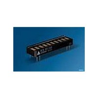
LED Displays 5x5 Super Red 0.145 , 10-CHARACTER
Manufacturer
OSRAM Opto Semiconductors Inc
Series
Intelligent Display®r
Datasheet
1.SCD55100A.pdf
(17 pages)
Specifications of SCD55102A
Display Type
Dot Matrix
Emitting Color
Hi-Eff. Red
Number Of Digits
10
Digit Size (in)
.145in
Viewing Area Height (mm)
3.68mm
Viewing Area Length (mm)
2.03mm
Package Type
Panel
Operating Supply Voltage (min)
4.5V
Operating Supply Voltage (typ)
5V
Operating Supply Voltage (max)
5.5V
Operating Temperature Classification
Industrial
Operating Temp Range
-40C to 85C
Mounting
Through Hole
Pin Count
10
Total Thickness (mm)
5.08mm
Opto Display Type
Panel
Pattern Type
Dot Matrix
Millicandela Rating
237µcd
Size / Dimension
1.50" L x 0.39" W x 0.20" H (38.10mm x 10.00mm x 5.08mm)
Color
Red
Configuration
5 x 5
Character Size
0.145 in
Illumination Color
High Efficiency Red
Wavelength
630 nm
Maximum Operating Temperature
+ 85 C
Minimum Operating Temperature
- 40 C
Luminous Intensity
237 ucd
Viewing Area (w X H)
2.03 mm x 3.68 mm
Lead Free Status / RoHS Status
Compliant
Voltage - Forward (vf) Typ
-
Internal Connection
-
Lead Free Status / Rohs Status
Lead free / RoHS Compliant
Other names
Q68100A0990


Pin Assignment
Pin
1
2
3
4
5
6
7
8
9
10
11
12
13
14
Switching Specifications
(over operating temperature range and V
Symbol
T
T
T
T
T
T
T
T
T
Note: T
Dot Matrix Format
2008-07-22
RC
LDS
DS
SDCLK
SDCW
LDH
DH
WR
BL
The SDCLK period must be a minimum of 200 ns.
SDCW
is the minimum time the SDCLK may be low or high.
Function
SDCLK
LOAD
NP
NP
NP
NP
NP
NP
NP
NP
NP
NP
RST
GND
Description
Reset Active Time
Load Setup Time
Data Setup Time
Clock Period
Clock Width
Load Hold Time
Data Hold Time
Total Write Time
Time Between Loads
Tolerance: ±0.25 (0.010)
SCD55100A, SCD55101A, SCD55102A, SCD55103A, SCD55104A
C0 C1 C2 C3 C4
0.56 (0.022) typ.
2.03 (0.080)
Pin
28
27
26
25
24
23
22
21
20
19
18
17
16
15
R0
R1
R3
R4
R5
IDOD5212
CC
=4.5 V to 5.5 V)
Function
GND
DATA
NP
NP
NP
NP
NP
NP
NP
V
NC
NP
CLKSEL
CLK I/O
Min.
600
50
50
200
70
0
25
2.2
600
CC
mm (inch)
Units
ns
ns
ns
ns
ns
ns
ns
μs
ns
6
Pin Definitions
Pin
1
2
3
4
5
6
7
8
9
10
11
12
13
14
15
16
17
18
19
20
21
22
23
24
25
26
27
28
Function
SDCLK
LOAD
NP
NP
NP
NP
NP
NP
NP
NP
NP
NP
RST
GND
CLK I/O
CLKSEL
NP
NC
V
NP
NP
NP
NP
NP
NP
NP
DATA
GND
CC
Definitions
Loads data into the 8-bit serial data register
on a low to high transition.
Low input enables data clocking into 8-bit
serial shift register. When LOAD goes high,
the contents of 8-bit serial Shift Register will
be decoded.
No Pin
No Pin
No Pin
No Pin
No pin
No pin
No Pin
No Pin
No Pin
No Pin
Asynchronous input, when low will clear the
Multiplex Counter, User RAM and Data
Register. Control Word Register is set to
100% brightness and the Address Register is
set to select Digit 0. The display is blanked.
Power supply ground
Outputs master clock or inputs external clock.
H=internal clock, L=external clock
No Pin
No connection
Power supply/heat sink
No Pin
No pin
No pin
No Pin
No Pin
No Pin
No Pin
Serial data input
Power supply ground
Related parts for SCD55102A
Image
Part Number
Description
Manufacturer
Datasheet
Request
R

Part Number:
Description:
Manufacturer:
OSRAM Opto Semiconductors Inc
Datasheet:

Part Number:
Description:
INTELLIGENT DISP 4CHAR 5X7 HERED
Manufacturer:
OSRAM Opto Semiconductors Inc
Datasheet:

Part Number:
Description:
DISPLAY 8DIGIT CERAMIC GREEN
Manufacturer:
OSRAM Opto Semiconductors Inc
Datasheet:

Part Number:
Description:
EMITTER IR 950NM 5MM SMD RADIAL
Manufacturer:
OSRAM Opto Semiconductors Inc
Datasheet:

Part Number:
Description:
LED TOPLED GREEN 570NM 2-PLCC
Manufacturer:
OSRAM Opto Semiconductors Inc
Datasheet:

Part Number:
Description:
INTERRUPTER RELFECT W/FILTR SMD
Manufacturer:
OSRAM Opto Semiconductors Inc
Datasheet:

Part Number:
Description:
LED Displays 5x7 Green 0.145 , 4-CHARACTER
Manufacturer:
OSRAM Opto Semiconductors Inc
Datasheet:
Part Number:
Description:
Q65110A4321_SIDELED PURE GREEN EOL150407
Manufacturer:
OSRAM Opto Semiconductors Inc
Datasheet:
Part Number:
Description:
Q65110A1202_RO DETECTOR 3/5MM_TR_RO
Manufacturer:
OSRAM Opto Semiconductors Inc
Datasheet:
Part Number:
Description:
INTELLIGENT DISP 4CHAR 5X7 HERED
Manufacturer:
OSRAM Opto Semiconductors Inc
Datasheet:
Part Number:
Description:
LED TOPLED GREEN 570NM 2-PLCC
Manufacturer:
OSRAM Opto Semiconductors Inc
Datasheet:

Part Number:
Description:
PHOTODIODE 900NM 3MM W/FILTER
Manufacturer:
OSRAM Opto Semiconductors Inc
Datasheet:

Part Number:
Description:
PHOTODIODE 850NM THRU-HOLE
Manufacturer:
OSRAM Opto Semiconductors Inc
Datasheet:

Part Number:
Description:
PHOTODIODE 880NM W/FILTER SMD
Manufacturer:
OSRAM Opto Semiconductors Inc
Datasheet: