HFCT-5963NG Avago Technologies US Inc., HFCT-5963NG Datasheet - Page 6
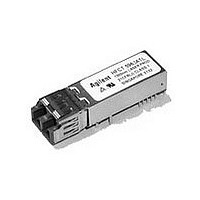
HFCT-5963NG
Manufacturer Part Number
HFCT-5963NG
Description
Manufacturer
Avago Technologies US Inc.
Datasheet
1.HFCT-5963NG.pdf
(16 pages)
Specifications of HFCT-5963NG
Optical Fiber Type
TX/RX
Data Transfer Rate
155Mbps
Optical Rise Time
2ns
Optical Fall Time
2ns
Operating Temperature Classification
Commercial
Peak Wavelength
1360/1580nm
Package Type
DIP With Connector
Operating Supply Voltage (min)
3.1V
Operating Supply Voltage (typ)
3.3V
Operating Supply Voltage (max)
3.5V
Output Current
50mA
Operating Temp Range
-5C to 70C
Mounting
Snap Fit To Panel
Pin Count
10
Lead Free Status / RoHS Status
Compliant


Connection Diagram
Pin Descriptions:
Pin 1 Receiver Signal Ground V
Directly connect this pin to the receiver ground plane.
Pin 2 Receiver Power Supply V
Provide +3.3 V dc via the recommended receiver power
supply filter circuit. Locate the power supply filter cir-
cuit as close as possible to the V
circuit should not cause V
specification.
Pin 3 Signal Detect SD:
Normal optical input levels to the receiver result in a
logic “1” output. Low optical input levels to the receiver
result in a logic “0” output. This Signal Detect output can
be used to drive a +3.3 V TTL input on an upstream cir-
cuit, such as Signal Detect input or Loss of Signal-bar.
Pin 4 Receiver Data Out Bar RD-:
No internal terminations are provided. See recommend-
ed circuit schematic.
Pin 5 Receiver Data Out RD+:
No internal terminations are provided. See recommend-
ed circuit schematic.
Pin 6 Transmitter Power Supply V
Provide +3.3 V dc via the recommended transmitter
power supply filter circuit. Locate the power supply fil-
ter circuit as close as possible to the V
6
RECEIVER SIGNAL GROUND
Figure 5. Pin Out Diagram (Top View)
RECEIVER POWER SUPPLY
RECEIVER DATA OUT BAR
RECEIVER DATA OUT
Grounding Tabs
SIGNAL DETECT
Package
o
o
o
o
o
CC
RX
CC
EE
1
2
3
4
5
RX:
to drop below minimum
View
RX:
Top
CC
CC
TX:
RX pin. Note: the filter
10
TX
9
8
7
6
CC
o
o
o
o
o
TX pin.
TRANSMITTER DATA IN BAR
TRANSMITTER DATA IN
TRANSMITTER DISABLE
TRANSMITTER SIGNAL GROUND
TRANSMITTER POWER SUPPLY
Mounting Studs/
Solder Posts
Pin 7 Transmitter Signal Ground V
Directly connect these pins to the transmitter signal
ground plane.
Pin 8 Transmitter Disable T
Optional feature, connect this pin to +3.3 V TTL logic
high “1” to disable module. To enable module connect
to TTL logic low “0”.
Pin 9 Transmitter Data In TD+:
No internal terminations are provided. See recommend-
ed circuit schematic.
Pin 10 Transmitter Data In Bar TD-:
No internal terminations are provided. See recommend-
ed circuit schematic.
Mounting Studs/Solder Posts
The two mounting studs are provided for transceiver
mechanical attachment to the circuit board. It is rec-
ommended that the holes in the circuit board be con-
nected to chassis ground.
Package Grounding Tabs
Connect four package grounding tabs to signal ground.
DIS
:
EE
TX:
Related parts for HFCT-5963NG
Image
Part Number
Description
Manufacturer
Datasheet
Request
R

Part Number:
Description:
TXRX SMF XFP 10BGE 2KM OC-192
Manufacturer:
Avago Technologies US Inc.
Datasheet:

Part Number:
Description:
Fiber Optic Transmitters, Receivers, Transceivers OC3 SFP IR -10 to +8 5 non-DMI
Manufacturer:
Avago Technologies US Inc.
Datasheet:

Part Number:
Description:
Fiber Optics, Transceiver Module
Manufacturer:
Avago Technologies US Inc.
Part Number:
Description:
Fiber Optic Transmitters, Receivers, Transceivers SFP OC12 IR Standard Delatch
Manufacturer:
Avago Technologies US Inc.

Part Number:
Description:
Manufacturer:
Avago Technologies
Datasheet:

Part Number:
Description:
155 Mb/s Single Mode Laser Transceiver For Atm, Sonet OC-3/SDH STM-1 (L1.1)
Manufacturer:
Agilent Technologies, Inc.
Datasheet:
Part Number:
Description:
Fiber Optics, Evaluation Kit
Manufacturer:
Avago Technologies US Inc.
Datasheet:
Part Number:
Description:
Fiber Optics, Evaluation Kit
Manufacturer:
Avago Technologies US Inc.
Datasheet:
Part Number:
Description:
Fiber Optics, Evaluation Kit
Manufacturer:
Avago Technologies US Inc.
Datasheet:

Part Number:
Description:
Agilent HFCT-5215B/D 155 Mb/s Single Mode Laser Transceiver
Manufacturer:
Hewlett-Packard
Datasheet:

Part Number:
Description:
OPTOCOUPLER GATE DRV 2A 16-SOIC
Manufacturer:
Avago Technologies US Inc.
Datasheet:
Part Number:
Description:
OPTOCOUPLER 2CH 2.5A 16-SOIC
Manufacturer:
Avago Technologies US Inc.
Datasheet:

Part Number:
Description:
OPTOCOUPLER GATE DRV 0.4A 16SOIC
Manufacturer:
Avago Technologies US Inc.
Datasheet:

Part Number:
Description:
OPTOCOUPLER 2.0A 250KHZ 8-DIP
Manufacturer:
Avago Technologies US Inc.
Datasheet:

Part Number:
Description:
OPTOCOUPLER 2.0A 250KHZ GW 8-SMD
Manufacturer:
Avago Technologies US Inc.
Datasheet: