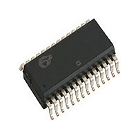
CY7C65113-SXC Cypress Semiconductor Corp, CY7C65113-SXC Datasheet - Page 20

CY7C65113-SXC
Manufacturer Part Number
CY7C65113-SXC
Description
Manufacturer
Cypress Semiconductor Corp
Datasheet
1.CY7C65113-SXC.pdf
(49 pages)
Specifications of CY7C65113-SXC
Operating Temperature (max)
70C
Operating Temperature (min)
0C
Operating Temperature Classification
Commercial
Package Type
SOIC
Mounting
Surface Mount
Lead Free Status / RoHS Status
Compliant
Available stocks
Company
Part Number
Manufacturer
Quantity
Price
Company:
Part Number:
CY7C65113-SXC
Manufacturer:
CYPRESS
Quantity:
770
Part Number:
CY7C65113-SXC
Manufacturer:
CYPRESS/赛普拉斯
Quantity:
20 000
Document #: 38-08002 Rev. *D
Bit [7:0]: Timer lower eight bits.
Bit [3:0]: Timer higher nibble
Bit [7:4]: Reserved.
11.0
Internal hardware supports communication with external devices through an I
discussed in detail in Section 12.0.
locations of the SCL (clock) and SDA (data) pins on Port 1 as shown in Table 11-1. These bits are cleared on reset. When the
GPIO is configured for I
on SCL and SDA is recommended.
.
Table 11-1. I
Note:
Bit #
Bit Name
Read/Write
Reset
Timer LSB
Bit #
Bit Name
Read/Write
Reset
I
Bit #
Bit Name
Read/Write
Reset
3.
Timer MSB
2
C Configuration
I
2
C-compatible function must be separately enabled, as described in Section 12.0.
I
2
C Position (Bit7, Figure 11-1)
I
2
C Configuration Register
11
L3
2
C Port Configuration
I
D3 D2 D1 D0 D7 D6 D5 D4 D3 D2 D1 D0
Timer Bit 7
2
Reserved
C Position
R/W
10 9
L2
R
7
0
7
–
0
7
0
0
2
C function, the internal pull ups on the pins are disabled. Addition of an external weak pull-up resistors
L1 L0
TimerBit 6
Reserved
Reserved
8
R/W
R
[3]
6
0
6
–
0
6
0
The I
7
2
Figure 11-1. I
C Position bit (Bit 7, Figure 11-1) and I
Timer Bit 5
6
Reserved
Reserved
Figure 10-3. Timer Block Diagram
Figure 10-2. Timer MSB Register
Figure 10-1. Timer LSB Register
R/W
R
5
0
5
–
0
5
0
I
2
C Port Width (Bit1, Figure 11-1)
5
2
4
C Configuration Register
Timer Bit 4
Reserved
Reserved
R/W
R
4
0
4
–
0
4
0
3
0
2
Timer Bit 11 Timer Bit 10
Timer Bit 3
Reserved
R/W
1
2
R
R
3
0
3
0
3
0
C-compatible interface. I
2
0
C Port Width bit (Bit 1, Figure 11-1) select the
8
Timer Bit 2
Reserved
R/W
R
R
2
0
2
0
2
0
1.024-ms interrupt
128-
I
2
1 MHz clock
To Timer Registers
C on P1[1:0], 0:SCL, 1:SDA
µ
s interrupt
Timer Bit 1
Timer Bit 9
I
2
I
2
2
C Position
C-compatible function is
Width
C Port
R/W
CY7C65113C
R
R
1
0
1
0
1
0
Address 0x24
Address 0x09
Address 0x25
Page 20 of 49
Timer Bit 0
Timer Bit 8
Reserved
R/W
R
R
0
0
0
0
0
0


