CY7C65113-SXC Cypress Semiconductor Corp, CY7C65113-SXC Datasheet - Page 8
CY7C65113-SXC
Manufacturer Part Number
CY7C65113-SXC
Description
Manufacturer
Cypress Semiconductor Corp
Datasheet
1.CY7C65113-SXC.pdf
(49 pages)
Specifications of CY7C65113-SXC
Operating Temperature (max)
70C
Operating Temperature (min)
0C
Operating Temperature Classification
Commercial
Package Type
SOIC
Mounting
Surface Mount
Lead Free Status / RoHS Status
Compliant
Available stocks
Company
Part Number
Manufacturer
Quantity
Price
Company:

Part Number:
CY7C65113-SXC
Manufacturer:
CYPRESS
Quantity:
770
Part Number:
CY7C65113-SXC
Manufacturer:
CYPRESS/赛普拉斯
Quantity:
20 000


Document #: 38-08002 Rev. *D
3.0
4.0
4.1
Table 4-1. Pin Assignments
D+[0], D–[0]
D+[1], D–[1]
D+[2], D–[2]
D+[3], D–[3]
D+[4], D–[4]
P0
P1
XTAL
XTAL
V
V
GND
V
PP
CC
REF
Name
IN
OUT
Pin Assignments
Pin Configurations
Product Summary Tables
OUT
I/O
I/O
I/O
I/O
I/O
I/O
I/O
I/O
IN
IN
5, 6
7, 8
9, 10
23, 24
21, 22
P1[7:0]
11, 15, 12, 16, 13, 17, 14, 18
P1[2:0]
25, 27, 26
2
1
19
28
4, 20
3
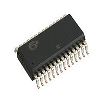
28-pin
XTALOUT
XTALIN
D+[0]
D+[1]
D+[2]
D–[0]
D–[1]
D–[2]
P0[7]
P0[5]
P0[3]
P0[1]
V
GND
REF
Upstream port, USB differential data.
Downstream Port 1, USB differential data.
Downstream Port 2, USB differential data.
Downstream Port 3, USB differential data.
Downstream Port 4, USB differential data.
GPIO Port 0 capable of sinking 7 mA (typical).
GPIO Port 1 capable of sinking 7 mA (typical).
6-MHz crystal or external clock input.
6-MHz crystal out.
Programming voltage supply, tie to ground during normal operation.
Voltage supply.
Ground.
External 3.3V supply voltage for the downstream differential data output
buffers and the D+ pull-up.
CY7C65113C
28-pin SOIC
Top View
1
2
3
4
5
6
7
8
9
10
11
12
13
14
28
27
26
25
24
23
22
21
20
19
18
17
16
15
V
P1[1]
P1[0]
P1[2]
D–[3]
D+[3]
D–[4]
D+[4]
GND
V
P0[0]
P0[2]
P0[4]
P0[6]
CC
PP
Description
CY7C65113C
Page 8 of 49
Related parts for CY7C65113-SXC
Image
Part Number
Description
Manufacturer
Datasheet
Request
R

Part Number:
Description:
Manufacturer:
Cypress Semiconductor Corp
Datasheet:
Part Number:
Description:
Manufacturer:
Cypress Semiconductor Corp
Datasheet:
Part Number:
Description:
Manufacturer:
Cypress Semiconductor Corp
Datasheet:
Part Number:
Description:
Manufacturer:
Cypress Semiconductor Corp
Datasheet:
Part Number:
Description:
Manufacturer:
Cypress Semiconductor Corp
Datasheet: