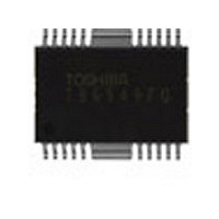
TB6549F Toshiba, TB6549F Datasheet - Page 10

TB6549F
Manufacturer Part Number
TB6549F
Description
Manufacturer
Toshiba
Datasheet
1.TB6549F.pdf
(22 pages)
Specifications of TB6549F
Operating Current
10mA
Operating Temperature Classification
Commercial
Package Type
HSOP
Operating Supply Voltage (min)
10V
Operating Supply Voltage (max)
27V
Lead Free Status / RoHS Status
Not Compliant
Available stocks
Company
Part Number
Manufacturer
Quantity
Price
Company:
Part Number:
TB6549F
Manufacturer:
TOSHIBA
Quantity:
5 510
Company:
Part Number:
TB6549FG
Manufacturer:
ROHM
Quantity:
15 000
Part Number:
TB6549FG
Manufacturer:
TOSHIBA/东芝
Quantity:
20 000
6. V
7. GND Sections
8. Power Monitoring Circuit
9. Thermal Shutdown (T
10. Overcurrent Detection (I
•
•
•
•
•
•
This IC includes a thermal shutdown circuit, which turns the output OFF when the junction temperature
(Tj) exceeds 160°C (typ.). The output turns back ON automatically. The thermal hysteresis is 20°C.
This IC includes a circuit to detect current flowing through the output power transistors. The current limit
is set to 5 A (typ.). The circuit detects a current flowing through each of the four output power transistors.
If the current in any one output power transistor exceeds the set limit, this circuit turns all the outputs
OFF.
This circuit includes a timer that causes the outputs to be OFF for 50 μs (typ.) after detection of an
overcurrent and then turn back ON automatically. If the overcurrent continues to flow, this ON-OFF
operation is repeated. Note that to prevent a malfunction due to a glitch, an insensitive period of 10 μs
(typ.) is provided.
The set limit is 5 A (typ.) as a design target value. The distributions shown below exist because of the
variations in thermal characteristics of different ICs. These distributions should be fully considered in the
motor torque design.
Also, output peak current should be less than 3 A because of the variations below,
CC
The V
circuit.
The operating voltage range is shown below:
This IC has a power monitoring function for preventing an output malfunction on power-up. However,
Toshiba recommends that IN1, IN2, and SB be set to the Low level at power-on.
This IC includes two separate GND sections: S-GND for controlling and P-GND for outputting. Be sure
to short-circuit these two GNDs as close to TB6549 as possible.
This circuit turns the output OFF when V
V
With a hysteresis of 0.3 V (design target value), the output turns back ON when V
(design target value) after this circuit starts operating.
Output Current
CC
Power Supply Section
= 4.6 V (typ.).
V
T
ΔT
Detected current: Approximately from 3.5 to 6.5 A
CC
SD
CC (opr.)
SD
power supply delivers a voltage to the output circuit, charge pump circuit, and internal 5 V
= 160°C (design target value)
= 20°C (design target value)
= 10 to 27 V
I
LIM
0
Insensitive period
SD
) Circuit
SD
10 μs
) Circuit
(typ.)
50 μs
(typ.)
reg
10 μs
(typ.)
10
becomes 3.0 V (design target value) or less. At this time,
50 μs
(typ.)
TB6549F/FG/P/PG/HQ
reg
exceeds 3.3 V
2007-3-6


