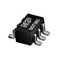
74AUP1T97GW NXP Semiconductors, 74AUP1T97GW Datasheet - Page 4

74AUP1T97GW
Manufacturer Part Number
74AUP1T97GW
Description
Manufacturer
NXP Semiconductors
Datasheet
1.74AUP1T97GW.pdf
(20 pages)
Specifications of 74AUP1T97GW
Logic Family
AUP
Technology
CMOS
High Level Output Current
-4mA
Low Level Output Current
4mA
Operating Supply Voltage (typ)
2.5/3.3V
Package Type
SOT-363
Operating Supply Voltage (max)
3.6V
Operating Supply Voltage (min)
2.3V
Abs. Propagation Delay Time
11.9ns
Mounting
Surface Mount
Pin Count
6
Operating Temperature (min)
-40C
Operating Temperature (max)
125C
Operating Temperature Classification
Automotive
Lead Free Status / RoHS Status
Compliant
NXP Semiconductors
Table 5.
74AUP1T97
Product data sheet
Logic function
2-input MUX
2-input AND
2-input OR with one input inverted
2-input NAND with one input inverted
2-input AND with one input inverted
2-input NOR with one input inverted
2-input OR
Inverter
Buffer
Fig 5.
Fig 7.
Fig 9.
B
A
C
2-input MUX
2-input NAND gate with input A inverted or
2-input OR gate with input C inverted
2-input OR gate
C
C
C
A
A
B
Function selection table
7.1 Logic configurations
Y
Y
Y
Y
A
B
B
A
1
2
3
1
2
3
1
2
3
6
5
4
6
5
4
All information provided in this document is subject to legal disclaimers.
6
5
4
001aae004
001aae006
001aae002
C
Y
C
Y
C
Y
V
V
CC
CC
V
CC
Rev. 2 — 18 October 2010
Low-power configurable gate with voltage-level translator
Figure
see
see
see
see
see
see
see
see
see
Fig 6.
Fig 8.
Fig 10. Inverter
Figure 5
Figure 6
Figure 7
Figure 7
Figure 8
Figure 8
Figure 9
Figure 10
Figure 11
2-input AND gate
2-input NOR gate with input B inverted or
2-input AND gate with input C inverted
C
C
C
A
B
B
C
Y
Y
Y
Y
A
B
1
2
3
74AUP1T97
1
2
3
1
2
3
6
5
4
001aae007
6
5
4
6
5
4
© NXP B.V. 2010. All rights reserved.
001aae003
001aae005
C
Y
V
C
Y
C
Y
CC
V
V
CC
CC
4 of 20


